

EPCS4SI8N Datasheet, Pinout, and Lot Verification Checks for OEM Buyers
EPCS4SI8N pinout, package, and datasheet limits buyers actually check — plus lot inspection notes. Request a quote on IC-Online; no invented stock claims.
Why EPCS4SI8N Configuration Flash Still Matters in Long-Life FPGA Designs
When an industrial motor drive ships with a fifteen-year service agreement, or a medical imaging system earns regulatory clearance after an eighteen-month validation cycle, the bill of materials becomes a locked-down document. Every component substitution—no matter how minor—can trigger costly re-qualification, firmware regressions, or worse, field failures that erode hard-won reliability reputations. This is the world where EPCS4SI8N continues to earn its place in procurement plans, even as newer configuration memories enter the market.
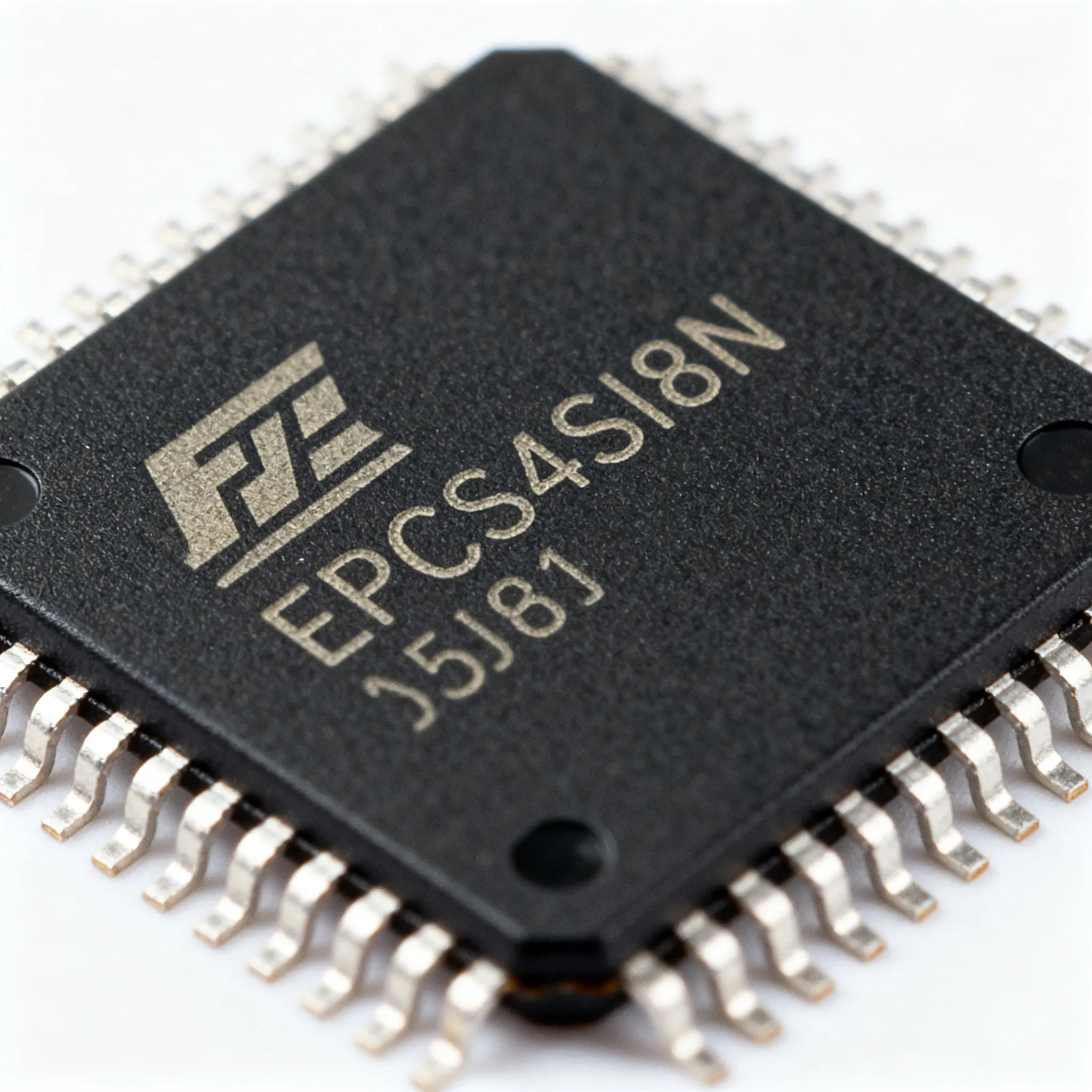
The EPCS4SI8N is Intel's (formerly Altera's) 4-Mbit serial configuration device, purpose-built to store FPGA bitstreams and deliver them reliably over the Active Serial (AS) interface. It sits in thousands of legacy Cyclone, Cyclone II, and Arria designs that remain in active production across industrial automation, defense systems, and medical instrumentation. Board respins for these platforms are measured in hundreds of thousands of dollars and months of regulatory paperwork—making the original configuration flash an enduring procurement requirement, not a legacy afterthought.
But longevity brings a parallel challenge: counterfeits. As EE Times has consistently documented, mature components with sustained OEM demand create the ideal conditions for sophisticated remarking operations. Configuration memories are particularly attractive targets because a non-functional or corrupted device won't always manifest as an immediate hard failure—it may produce intermittent boot failures, configuration errors at temperature extremes, or silent data corruption that evades factory test but surfaces in the field months later. For the procurement professional sourcing EPCS4SI8N, datasheet literacy and lot verification are no longer optional due diligence steps; they are the minimum barrier between a reliable production line and a costly recall.
The purpose of this article is to give electronics engineers and OEM buyers a single reference that bridges the technical and procurement domains: the electrical specifications that matter for design validation, the pinout and protocol details that govern board-level integration, a candid comparison with alternative configuration flash paths, and a concrete lot verification workflow that can be executed at incoming inspection. Every recommendation is grounded in manufacturer documentation and industry-standard practices, drawing on IPC Standards for component acceptance criteria where applicable.
Key Takeaway: EPCS4SI8N remains a critical line item for OEMs sustaining long-life FPGA-based systems. A disciplined approach to specification review and authenticity verification protects against the twin risks of design incompatibility and counterfeit infiltration—both of which carry costs far exceeding the unit price of the memory chip itself.
Decoding the EPCS4SI8N Datasheet: Memory Map, Active Serial Protocol, and Pinout
Before evaluating any sourcing decision around EPCS4SI8N, the engineering team must be grounded in what the datasheet actually specifies. The device is a 4-Mbit serial flash memory organized as 2,097,152 bits of user-accessible configuration storage, accessed through a dedicated Active Serial x1 interface. It is not a general-purpose SPI flash device, and treating it as such is one of the most common mistakes made during component crisis substitution exercises.
The EPCS4SI8N operates from a single 2.7 V to 3.6 V supply rail, packaged in an 8-pin narrow-body SOIC (150-mil body width). The pin count is minimal, but each signal carries specific timing and signal-integrity requirements that influence PCB layout decisions—especially trace length matching on DCLK and DATA lines, and proper decoupling at the VCC pin. Below are the essential electrical and functional parameters extracted from Intel's configuration device documentation.
| Parameter | Value | Unit / Notes |
|---|---|---|
| Density | 4 Mbit (512 K × 8) | Organized for FPGA bitstream storage |
| Supply Voltage (VCC) | 2.7 – 3.6 | V; single-supply operation |
| Standby Current (ISB) | 50 (typ.) | µA; low-power state when nCS is high |
| Active Current (ICC1) | 10 (typ. at 40 MHz) | mA; during sequential read |
| Maximum DCLK Frequency | 40 | MHz; Active Serial x1 read clock |
| Interface Protocol | Active Serial (AS) x1 | Not standard SPI; Altera/Intel proprietary command set |
| Page Size | 256 | Bytes; page-write buffer |
| Sector Size | 64 | KB; erase granularity |
| Write Endurance | 100,000 | Cycles per sector (typical) |
| Data Retention | 20 | Years at typical operating conditions |
| Package | 8-pin SOIC (150-mil) | Pb-free, RoHS-compliant; suffix "N" |
| Operating Temperature Range | -40 to +85 | °C; industrial grade |
The 40 MHz DCLK ceiling sets an upper bound on configuration speed. In practice, many designs clock the AS interface conservatively at 20–30 MHz to preserve signal integrity across longer board traces or in electrically noisy environments. The 256-byte page buffer means that programming operations must respect page boundaries; crossing a page boundary without issuing a new write command will cause data wrap-around within the same page—a subtle failure mode that has trapped more than one engineer during bootloader development.
Pin Functions and Signal Flow
The EPCS4SI8N pinout follows the standard 8-pin SOIC assignment familiar to engineers who have worked with the EPCS family. Each pin's role is tightly coupled to the AS state machine inside the FPGA, and signal direction depends on whether the device is being read (configuration download) or written (programming). The following table maps each pin to its function during normal AS read operation.
| Pin Number | Pin Name | Direction (AS Read) | Function Summary |
|---|---|---|---|
| 1 | nCS | Input (from FPGA) | Chip select; active low. De-asserting nCS terminates any ongoing operation. |
| 2 | DATA | Output (to FPGA) | Serial data output; configuration bitstream driven on DCLK falling edge. |
| 3 | VCC | — | 2.7–3.6 V supply; place 0.1 µF decoupling capacitor within 5 mm of pin. |
| 4 | GND | — | Common ground; tie directly to PCB ground plane. |
| 5 | ASDI | Input (from FPGA) | Active Serial Data Input; programming data and commands from FPGA. |
| 6 | DCLK | Input (from FPGA) | Configuration clock; data latched and driven on opposite edges. |
| 7 | NC | — | No connect; leave floating or tie to GND per layout guidelines. |
| 8 | NC | — | No connect; leave floating or tie to GND per layout guidelines. |
Two layout considerations deserve emphasis. First, the DCLK and DATA traces should be treated as a source-synchronous pair with matched length routing wherever possible—skew exceeding a few hundred picoseconds can erode timing margin at 40 MHz, especially at elevated temperatures. Second, the VCC decoupling capacitor must be placed as close as feasible to pins 3 and 4; Intel's characterization data assumes a low-inductance supply path, and excessive supply bounce during read operations can manifest as intermittent bit errors that are notoriously difficult to diagnose. These assembly and layout practices align with IPC-A-610 workmanship standards for surface-mount component acceptance.
Tip: When reviewing legacy schematics that use EPCS4SI8N, confirm that the FPGA's MSEL pins are strapped for Active Serial (AS) mode, not Active Serial ×4 (AS×4) or JTAG-only configuration. A mismatch here will prevent the FPGA from toggling DCLK and nCS correctly, leading to a blank "configuration failed" state that is easily misattributed to a faulty memory device.
Alternatives to EPCS4SI8N: EPCQ-L, Standard SPI Flash, and When Migration Makes Sense
Every procurement team managing long-lifecycle FPGA products eventually faces the same question: can we substitute EPCS4SI8N with something more readily available, less expensive, or from a multi-sourced supply base? The answer depends on the FPGA generation, the configuration mode, and the risk appetite of the organization. This section compares three categories of configuration storage—the original EPCS device, Intel's newer EPCQ-L series, and a representative standard SPI NOR flash—across the dimensions that matter for both engineering and sourcing decisions.
| Comparison Metric | EPCS4SI8N (Intel EPCS) | Intel EPCQ-L (e.g., EPCQ4A) | Standard SPI NOR (e.g., Winbond W25Q40) | Selection Criteria & Failure Boundary |
|---|---|---|---|---|
| Command Set | Proprietary Active Serial command set | Extended AS command set with AS×4 support | Standard SPI command set (03h, 0Bh, etc.) | FPGA AS controller expects EPCS opcodes; standard SPI flash may not respond to AS read commands. |
| Maximum Interface Speed | 40 MHz (AS×1) | 100+ MHz (AS×4 capable) | 104 MHz (standard SPI, Quad-SPI capable) | Speed advantage only relevant if FPGA supports faster modes and board layout permits. |
| Supply Voltage | 2.7–3.6 V | 2.7–3.6 V (single supply) | 2.7–3.6 V (wide-voltage variants available) | Voltage compatibility is straightforward; all three operate in overlapping ranges. |
| Active Serial (AS) Mode Support | Native, fully compatible | Native, with AS×4 on supported FPGAs | Not supported in dedicated AS mode; requires FPGA SPI master or JTAG indirect programming | Critical: Standard SPI flash cannot replace EPCS in true AS mode without FPGA controller redesign. |
| Sector Architecture | 64 KB uniform sectors | 64 KB uniform sectors | 4 KB / 32 KB / 64 KB (mixed, device-dependent) | Bitstream placement must respect sector boundaries; mixed-size sectors complicate software. |
| Package Footprint | 8-pin SOIC (150-mil) | 8-pin SOIC or 8-pin DFN | 8-pin SOIC (150/208-mil), WSON, USON | Verify exact land pattern; SOIC-8 variations exist in body width. |
| Supply Chain Profile | Single-source (Intel), mature product | Single-source (Intel), active production | Multi-sourced (Winbond, Macronix, GigaDevice, etc.) | Multi-source SPI flash offers supply-chain diversity; verify FPGA configuration controller compatibility first. |
The comparison reveals a fundamental architectural constraint: EPCS4SI8N uses a proprietary Active Serial command sequence that is not a subset of the standard SPI instruction set. An FPGA strapped for AS mode issues specific read commands and expects specific status register responses that a general-purpose SPI NOR flash like the Winbond W25Q40 simply does not implement. This isn't a minor firmware tweak—it is a hardware protocol incompatibility at the FPGA configuration controller level.
However, some FPGA families—particularly Intel's Cyclone III and later devices—support a generic "ASMI" (Active Serial Memory Interface) or SPI master mode that can be configured to work with standard SPI flash. Similarly, the EPCQ-L series from Intel offers a migration path within the same manufacturer ecosystem, supporting the original AS command set for backward compatibility while adding AS×4 capability for faster configuration on newer FPGAs. The key action for any engineering team evaluating a substitution is to pull the FPGA family datasheet, locate the configuration mode table, and verify whether the target FPGA's MSEL strapping options include a mode compatible with the candidate flash device.
Note: Even when an FPGA technically supports a generic SPI configuration mode, the board-level pinout may not be electrically compatible without PCB modifications. The ASDI pin on EPCS4SI8N, for instance, maps to a specific FPGA I/O that may not be the same pin used for MOSI in a generic SPI mode. Always cross-check the FPGA pin table against the existing schematic before declaring a substitution electrically viable.
Lot Verification Steps for OEM Buyers: Authenticating EPCS4SI8N Chips Before Board Assembly
A component that costs a few dollars at the unit level can destroy tens of thousands of dollars in value if it turns out to be counterfeit, reclaimed, or remarked. For configuration memories like EPCS4SI8N, the failure mode is particularly insidious: a device may program and verify correctly at room temperature, pass automated optical inspection, and still harbor latent defects—thinned oxide layers from die recovery, incorrect sector maps from a remarked lower-density part, or degraded charge pumps that fail after a few hundred thermal cycles. The incoming inspection workflow needs to catch what automated test may miss.
The verification steps below are adapted from industry-standard counterfeit detection practices and align with the visual acceptance criteria documented in IPC-A-610. They are ordered from the fastest and lowest-cost checks to more involved techniques that make sense for higher-volume or higher-criticality lots.
| Verification Step | Method | Pass Criteria | Red Flags |
|---|---|---|---|
| 1. Visual Inspection (10× Magnification) | Examine top-side markings, mold texture, and pin-1 indent under a stereo microscope with oblique lighting. | Consistent mold texture across all units in the lot; laser-etched markings with crisp edges; uniform indent geometry. | Sanding or grinding marks on the package surface; inconsistent indents (dot vs. dimple); ghost markings visible under low-angle light. |
| 2. Acetone Wipe Test | Apply a cotton swab saturated with acetone to the top marking; rub gently for 10 seconds; inspect for smearing. | Marking remains intact and legible with no visible degradation. | Marking dissolves, smears, or lifts—indicative of blacktopping and re-marking over an original component. |
| 3. Date Code Coherence | Cross-reference the 4-digit date code (YYWW format) on the component against Intel's publicly documented last-time-buy and EOL notices for EPCS4SI8N. | Date code falls within the known active production window; lot code format matches Intel's conventions. | Date codes after the last-time-buy window; date codes that don't follow Intel's formatting convention; mixed date codes within a single sealed package. |
| 4. JEDEC Manufacturer ID Read (9Fh) | Using an SPI programmer or FPGA-based test fixture, issue the JEDEC Read ID command (9Fh) and capture the manufacturer ID byte. | Returns the expected Altera/Intel manufacturer code consistent with EPCS family devices. | Returns an unexpected manufacturer code (e.g., a commodity SPI flash vendor ID) or all-zeros/all-ones response. |
| 5. Packaging Label Audit | Examine the outer box, inner reel/tray labels, and moisture-barrier bag for consistency. Verify label format, font, and traceability information against known Intel packaging standards. | Labels are consistent across packaging layers; lot codes match; moisture indicator card shows appropriate humidity exposure. | Mismatched lot codes between inner and outer packaging; labels with non-standard fonts or alignment; missing or altered moisture-barrier bag seals. |
| 6. X-ray or SAM (for high-value lots) | Perform 2D X-ray imaging or Scanning Acoustic Microscopy on a sample from the lot to examine die size, lead-frame integrity, and die-attach consistency. | Consistent die size and orientation across samples; no voids or delamination in die-attach; lead-frame geometry matches known-good reference. | Inconsistent die sizes suggesting mixed-origin components; die-attach voids or delamination indicative of reclaimed dice. |
Steps 1 through 4 can be performed at most OEM incoming inspection stations with minimal investment beyond a stereo microscope, acetone, and a basic SPI test jig. Steps 5 and 6 involve more specialized equipment and are typically reserved for larger lot sizes, safety-critical assemblies, or instances where earlier visual checks have raised suspicion. As EE Times reporting on counterfeit electronics has documented, the most sophisticated remarking operations can defeat visual and solvent-based tests alone, making electrical verification (Step 4) the essential gate that separates a convincing cosmetic job from a functionally authentic device.
Tip: Build a known-good reference library. Retain two or three verified-authentic EPCS4SI8N units from an authorized distributor shipment and photograph them at high resolution under consistent lighting. These reference images—showing the exact mold texture, marking font, indent shape, and pin-1 chamfer—become invaluable comparison tools when evaluating lots from unfamiliar sources. The human eye is remarkably good at spotting deviations from a memorized reference, and this simple practice costs nothing.
EPCS4SI8N Sourcing and Design Questions Engineers and Buyers Ask
The boundary between engineering and procurement is where configuration memory sourcing decisions get complicated. The questions below represent the real conversations happening in design reviews and purchasing meetings—spanning authenticity, compatibility, endurance, and lifecycle management. Each answer is written to be actionable for both technical and commercial stakeholders.
Q: How can I authenticate an EPCS4SI8N lot and spot counterfeit or reclaimed units?
Start with a visual inspection under 10× magnification, looking for surface texturing inconsistencies, sanding marks, or irregular pin-1 indents. Apply an acetone wipe to the top marking—if the marking smears or dissolves, blacktopping is virtually certain. Verify the date code against Intel's publicly documented last-time-buy dates for the EPCS family; any date code that post-dates the known active production window demands an explanation. Electrically, issue the JEDEC manufacturer ID read command (9Fh) over SPI to confirm the device returns the expected Altera/Intel manufacturer code. For high-volume or high-criticality lots, cross-reference packaging labels across all layers—outer carton, inner reel, and moisture-barrier bag—and consider X-ray or Scanning Acoustic Microscopy to examine die consistency and lead-frame geometry. Each of these steps adds a layer of confidence; no single check is sufficient on its own.
Q: Can I drop a standard 4-Mbit SPI NOR flash like W25Q40 onto my board in place of EPCS4SI8N?
Not without careful verification, and in many legacy designs, not at all. The EPCS4SI8N uses the Active Serial (AS) protocol with a proprietary command set; Altera and early Intel FPGAs configured in AS mode issue read commands and expect status responses that standard SPI NOR flash devices do not implement. Some newer FPGA families—Cyclone III and later—support a generic SPI master configuration mode that can interface with commodity SPI flash, but this requires the FPGA's MSEL pins to be strapped appropriately and the configuration controller to be configured for standard SPI command sequences. Even when the FPGA supports it, the board-level pin mapping may not align without a PCB change. Always consult the specific FPGA family datasheet and verify the configuration controller requirements before attempting any substitution. Treat any "compatibility must be verified (package, pinout, firmware)" claim with skepticism and demand board-level boot testing across temperature corners.
Q: What are the typical data retention and write endurance for EPCS4SI8N?
Intel's characterization data specifies 20-year data retention and 100,000 write cycles per sector under typical operating conditions (nominal voltage, specified temperature range). These are silicon-level endurance figures; real-world longevity depends on operating temperature, supply voltage stability, and the frequency of configuration updates. In applications where the FPGA bitstream is written once at factory test and read at every power-up—the most common usage model—the write endurance limit is rarely approached. For designs that perform in-field firmware updates, consider worst-case temperature and voltage margins when planning the update cadence. A device operating continuously at 85°C will have a shorter data retention horizon than one at 25°C; Intel's application notes provide detailed acceleration models for engineers performing reliability budgeting.
Q: Does EPCS4SI8N need to be pre-programmed before PCB assembly?
Not necessarily. A blank device can be programmed in-system through the JTAG chain via the FPGA, using the Active Serial programming mode supported by Intel's Quartus programming tools. The FPGA acts as a bridge, receiving the configuration bitstream over JTAG and forwarding it to the EPCS device over the AS interface. However, many OEMs opt to pre-program configuration memories off-board for two practical reasons: it eliminates in-system programming time from the production line takt time, and it ensures that every assembled board powers up into a known-good configuration on first boot—simplifying functional test and reducing diagnostic time. Pre-programming also enables the use of socketed programmers that can verify write integrity at elevated temperature, something that is more difficult to achieve after soldering. If your contract manufacturer offers pre-programming as a value-added service, weigh the per-unit cost against the line-time savings and diagnostic simplification it provides.
Q: What is the difference between EPCS4SI8N and EPCS4SI8G?
The trailing letter in the ordering suffix indicates package material composition and environmental compliance level. The 'N' suffix designates a Pb-free (RoHS-compliant) SOIC package with matte tin plating, which is the standard option for most modern assembly processes. The 'G' suffix typically denotes a "green" initiative variant with specific halogen-free or low-halogen material sets that may be required for certain OEM environmental compliance programs. Electrically and functionally, the two variants are identical—same density, same timing, same command set. The difference is restricted to package material composition. Always cross-reference the exact ordering suffix against the Intel FPGA Configuration Devices ordering information document to confirm the material declaration aligns with your assembly process and corporate environmental compliance requirements. Ordering the wrong suffix can create a compliance audit finding even if the device works perfectly on the board.
Q: How should I handle lot verification if EPCS4SI8N is already discontinued?
Even as a mature device, EPCS4SI8N may still be available through authorized distributors that hold last-time-buy inventory or through OEM excess programs. When sourcing discontinued parts, elevate your verification rigor. Source only from authorized channels with documented chain-of-custody—unauthorized or gray-market sources multiply the counterfeit risk exponentially for EOL components. Perform the full suite of incoming inspection steps: visual inspection, acetone wipe, date-code coherence check, JEDEC ID read, and packaging label audit as a minimum baseline. For safety-critical or high-reliability applications, engage a third-party test laboratory for detailed authenticity reporting, including decapsulation and die-level analysis if warranted. Maintain strict lot traceability so that any field failures can be linked to a specific purchase event and supplier. If the verification results raise any doubt, quarantine the lot and escalate—the cost of a false positive (rejecting a good lot) is a sourcing delay; the cost of a false negative (accepting counterfeits) is measured in field failures and reputational damage.
The sourcing landscape for mature configuration memories rewards diligence and penalizes shortcuts. Whether you are procuring EPCS4SI8N for an ongoing production run or qualifying a last-time-buy lot for a product entering its sustainment phase, the combination of datasheet knowledge, verification discipline, and supplier scrutiny separates reliable supply lines from costly surprises. For a comprehensive bill of materials that includes configuration flash, FPGA, and supporting passives, a streamlined RFQ process that handles mixed-BOM requirements and flexible minimum order quantities can compress the sourcing cycle without compromising on the verification steps described above.
To request current pricing, confirm allocation status, or upload a complete bill of materials for a consolidated quote, visit IC-Online. The platform supports mixed-BOM RFQs with flexible MOQ terms, enabling procurement teams to address configuration memory sourcing alongside the broader component requirements of long-lifecycle FPGA designs.
References & Further Reading
Related Articles
 Blog
What Arduino Simulators Do for Electronic Functionality
Arduino simulators emulate boards and components to test code and circuits virtually. They replicate pin states, signals, and protocols for faster debugging.
 Blog
Exhaust Resonator vs Muffler Understanding the Key Differences
An exhaust resonator tunes specific sound frequencies to cancel drone and rasp, while a muffler reduces overall volume. Learn how each shapes your car's sound.
 Blog
Counterfeit IC Risk Mitigation for Procurement Teams: Lot Verification, ERAI, and Traceability Documents
How OEM buyers inspect suspect lots, request traceability, and escalate ERAI risk — a procurement checklist, not a hobby explainer.
 Blog
Power Sequencer IC or Discrete Sequencing? Critical RFQ Verification Steps for OEM Power Rails
Buyer-side specification, inspection, and RFQ checks on this technical topic. Not a hobby explainer. Request a quote on IC-Online.
 Blog
How Resonators Improve Your Exhaust Sound
What do resonators do in an exhaust system? They cancel specific frequencies to reduce drone and refine tone, improving your exhaust sound without adding volume.
 Blog
What Is Diode Polarity? Anode and Cathode Guide
Diode polarity: the anode is positive, cathode negative. Current flows anode to cathode. Learn to identify diode positive and negative terminals.