How OSAT Services Drive Electronics Innovation
OSAT stands for outsourced semiconductor assembly and test. These services form the backbone of the modern electro
OSAT stands for outsourced semiconductor assembly and test. These services form the backbone of the modern electronics industry. An OSAT provider enables companies to bring smaller and more powerful devices to market faster. This process makes innovations in smartphones, wearables, and AI hardware possible for everyone. The growing OSAT market shows its importance in the semiconductor world.
| Year | Market Size (USD Billion) |
|---|---|
| 2025 | 52.59 |
| 2033 | 101.01 |
The projected Compound Annual Growth Rate (CAGR) from 2025 to 2033 is 8.5%.
Key Takeaways
- OSAT companies turn raw chips into finished parts for electronics. They make devices smaller and more powerful.
- Advanced packaging methods like SiP and 3D stacking help make devices tiny and fast. This is important for phones and AI.
- OSAT companies test every chip to make sure it works well and lasts a long time. This ensures good quality.
- Using OSAT services helps companies save money and get products to stores faster. This makes electronics more affordable for everyone.
Advanced Packaging: The Core of OSAT Innovation
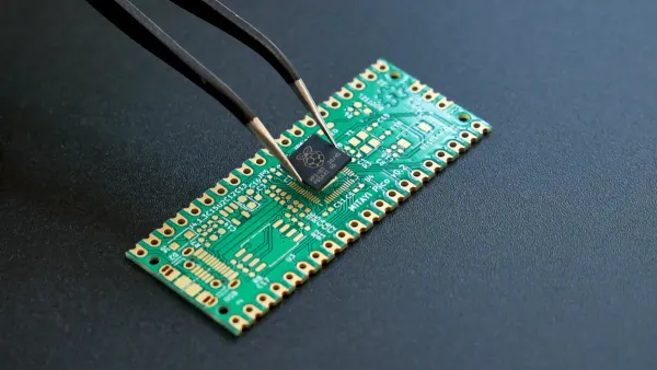
The magic of modern electronics happens after a chip is made. OSAT providers take these raw silicon wafers and transform them into finished components. They achieve this through advanced packaging solutions. This process involves placing one or more semiconductor chips into a single, protective casing that connects to the final device. This packaging is not just a box; it is a critical piece of engineering that defines a device's size, speed, and power efficiency.
Different packaging methods serve different needs. The market shows a clear preference for certain types based on their capabilities.
| Packaging Type | Market Share (2024) | CAGR (Forecast Period) |
|---|---|---|
| Ball Grid Array (BGA) | 42.5% | 8.1% |
| Chip Scale Packaging (CSP) | N/A | 10.5% |
This data highlights how established technologies like BGA remain dominant while newer, more compact forms like CSP are growing faster. OSAT companies are at the forefront of developing and implementing these advanced techniques.
System-in-Package (SiP) for Miniaturization
System-in-Package (SiP) technology is a primary driver of miniaturization. It allows an OSAT to integrate a full electronic system into one package. This includes the processor, memory, sensors, and communication modules. The result is a powerful, multi-functional chip in an incredibly small footprint.
The consumer electronics industry heavily relies on SiP. It enables the sleek designs of our favorite gadgets.
- Smartphones: The Samsung Galaxy S25 series uses SiP to fit its 5G antenna and other parts into a package 15% smaller than before.
- Wearables: The Apple Watch Series 10 integrates its processor, sensors, and radio into a SiP that is 20% thinner than previous versions. This technology is essential for making wearables small and comfortable enough for daily use.
💡 Did You Know? SiP is also crucial for the Internet of Things (IoT). It allows for the creation of tiny, low-power sensors and modules used in smart homes, industrial control systems, and even bionic arms for children. Some Bluetooth SiP modules are as small as 8x8 mm.
2.5D and 3D Packaging for Peak Performance
While SiP shrinks devices, 2.5D and 3D packaging technologies push their performance to the maximum. These methods focus on shortening the distance that data must travel between different chips, which increases speed and reduces power consumption.
2.5D packaging places chips side-by-side on a silicon base called an "interposer." This interposer contains ultra-fine wiring that connects the chips. 3D packaging takes this a step further by stacking chips vertically and connecting them with tiny vertical wires called Through-Silicon Vias (TSVs). This vertical stacking creates the shortest possible path for data.
| Aspect | 2.5D Packaging | 3D-IC Packaging |
|---|---|---|
| Bandwidth | Very high | Highest |
| Latency | Low | Minimal |
This leap in performance is critical for demanding applications like Artificial Intelligence (AI) and high-performance computing. For example, advanced GPUs from NVIDIA and AMD use these techniques to place high-bandwidth memory (HBM) right next to the main processor. This close integration feeds the processor data at incredible speeds, which is essential for training complex AI models. Building these high-performance semiconductor components requires deep expertise. This is why leading chip designers often work with designated partners. For instance, Nova Technology Company (HK) Limited is a HiSilicon-designated solutions partner, helping to bring such complex designs to life.
Fan-Out Wafer-Level Packaging (FOWLP)
Fan-Out Wafer-Level Packaging (FOWLP) offers a balance of performance, size, and cost. In this technique, a chip is placed on a wafer and encased in an epoxy mold. The electrical connections are then "fanned out" from the chip onto the surface of the mold, creating more space for connections than the chip itself allows.
This approach provides several key benefits over traditional methods:
- Better Performance: Shorter connections improve electrical and thermal performance, making it ideal for high-frequency parts.
- Thinner Packages: Eliminating layers makes the final component thinner and lighter.
- Lower Cost: The process is more economical for achieving high connection density.
Because of these advantages, FOWLP is the preferred packaging for many types of chips. It is especially useful for RF transceivers, baseband processors, and power management ICs. These components are vital in smartphones, communication infrastructure, and even electric vehicles, where efficiency and reliability are paramount.
The Role of Outsourced Semiconductor Assembly and Test
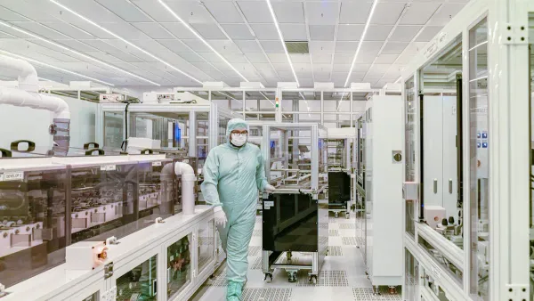
Advanced packaging creates the physical chip, but the work of an OSAT provider does not stop there. The second half of outsourced semiconductor assembly and test is just as important. After assembly, an OSAT provider must test every chip. This critical step ensures each component functions perfectly before it reaches the consumer. This process guarantees quality and reliability for the entire semiconductor market.
Ensuring Quality with Final Electrical Testing
Final electrical testing confirms that a chip works as designed. OSAT companies use Automated Test Equipment (ATE) to perform these checks. These advanced testing methodologies verify many aspects of chip performance. Key tests include:
- Functional Tests: These check that the chip performs its basic tasks correctly.
- DC Parametric Tests: This process measures voltage and current to find any shorts or opens.
- At-Speed Scan Testing: This test runs the chip at its operational speed to find timing-related flaws.
This detailed screening catches defects early. It ensures that only high-quality, functional chips are sent to device manufacturers.
Stress and Burn-in Testing for Reliability
A chip must not only work, but it must also last. OSATs use stress and burn-in testing to ensure long-term reliability. Burn-in testing subjects chips to high temperatures, often around 125°C, for 48 to 168 hours. This process weeds out weak components that would fail early in their life.
Stress tests simulate real-world conditions. A chip might experience rapid temperature changes from -65°C to +150°C to check for cracks or material failures.
These reliability tests follow strict industry standards. Organizations like JEDEC provide guidelines, such as the JESD47 standard for stress-test qualification, to ensure consistent quality across all electronic devices.
Accelerating Time-to-Market with Efficient Screening
Testing millions of chips requires incredible speed and precision. An OSAT achieves this using highly automated screening and sorting technologies. Machines like pick-and-place or turret sorters can process over 100,000 units per hour.
Many of these systems now use AI-based vision to spot defects that are invisible to the human eye. This automation allows an OSAT to screen massive volumes of chips quickly and accurately. This efficiency helps companies get their products from the design phase to store shelves much faster.
Driving the OSAT Market and Lowering Costs
The business model of outsourced semiconductor assembly and test is a key reason for the rapid growth of the electronics industry. OSAT providers create a system that lowers costs and removes major barriers for innovators. This approach makes advanced technology more affordable and accessible to everyone.
Lowering Barriers for Fabless Innovators
Building a semiconductor assembly and testing facility costs billions of dollars. This high cost stops many new companies from entering the market. The OSAT model offers a solution. Fabless companies can focus on designing innovative chips without needing to build their own factories. They outsource the expensive manufacturing and testing stages to an OSAT partner. This business strategy creates huge market opportunities for development.
This partnership significantly reduces operational expenses. A company can save over 70% on development costs by outsourcing. For example, the fabless innovator Astera Labs ships millions of units by integrating its systems directly with its OSAT partners. This frees up internal resources and allows them to scale quickly. Solution providers also play a role in this ecosystem. For instance, Nova Technology Company (HK) Limited, a HiSilicon-designated solutions partner, helps fabless companies navigate the complex path from chip design to final production.
Creating Economies of Scale for Affordability
OSAT companies handle enormous production volumes from hundreds of clients. This massive scale creates economies of scale, which lowers the per-unit cost for everyone. The OSAT market is dominated by a few large players who process billions of chips annually.
This high volume allows an OSAT to invest in cutting-edge equipment that improves efficiency. For example, adopting panel-level processing can reduce packaging costs by 25%. This continuous drive for efficiency, fueled by demand from consumer electronics, directly translates into more affordable smartphones, laptops, and other gadgets for end-users. This affordability is a major factor in the market's continued growth.
Making Advanced Electronics an Appropriate Technology
The cost reductions driven by OSAT services help make advanced electronics an appropriate technology for a wider range of applications. An appropriate technology is one that is suitable for the social and economic conditions of a community. By making powerful chips affordable, the OSAT model supports this idea. It enables the creation of low-cost computing devices for schools and networking solutions for developing regions.
This accessibility fosters innovation in areas like open-source hardware and open design. When components are cheaper, more people can experiment and build new products. This aligns with the principles of open-source appropriate technology, which promotes shared knowledge and community-driven solutions. Furthermore, the efficiency of the OSAT model contributes to sustainability. More efficient chips consume less power, supporting sustainable development goals and the creation of environmentally sound products, including those used in renewable energy systems. This makes open-source technology more viable for a better future.
OSAT providers fuel innovation through three core contributions. They enable physical miniaturization with advanced packaging, guarantee product quality through rigorous testing, and accelerate the entire industry with a cost-effective business model. The industry's shift toward chiplets and heterogeneous integration only increases the importance of the OSAT model.
This makes the outsourced semiconductor assembly and test (OSAT) market an unseen but essential engine. Ultimately, the work of an osat ensures the powerful and reliable electronics we depend on every day are possible.
FAQ
What does an OSAT company do?
An OSAT company provides outsourced semiconductor assembly and test services. It takes finished silicon wafers from a chip designer. The company then assembles them into protective packages and performs rigorous testing to ensure quality and reliability before the chips go into electronic devices.
What is the difference between assembly and testing?
Assembly is the physical process of putting a chip into a package. This package protects the chip and connects it to a device. Testing is the electrical screening process. It verifies that the chip functions correctly and will last a long time.
Why do companies use OSAT services?
Companies use OSAT services to lower costs and speed up production. Building assembly and test factories is very expensive. Outsourcing allows fabless companies to focus their money and effort on designing innovative new chips, helping them bring products to market faster.
How does advanced packaging help my devices?
Advanced packaging makes your devices smaller and more powerful. Techniques like SiP and FOWLP allow manufacturers to fit more functions into a tiny space. This innovation leads to thinner smartphones, smaller wearables, and more efficient performance in all modern electronics.