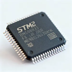
Semiconductor Advanced Packaging Heats Up Amid Industry Competition
As semiconductor technology continues to evolve, advanced packaging has emerged as a critical battleground for industry leaders. The need for higher interconnect density and process integration has driven substantial investments from key players. Companies such as Powertech Technology (PTI), Amkor, Unisoc, and ZhiJu Semiconductor are ramping up production, while TSMC and Samsung continue to push technological advancements. With increasing competition, the advanced packaging sector is witnessing rapid innovation and market expansion.
The Rising Battlefield in Semiconductor Advanced Packaging
As semiconductor technology continues to evolve, advanced packaging has emerged as a critical battleground for industry leaders. The need for higher interconnect density and process integration has driven substantial investments from key players. Companies such as Powertech Technology (PTI), Amkor, Unisoc, and ZhiJu Semiconductor are ramping up production, while TSMC and Samsung continue to push technological advancements. With increasing competition, the advanced packaging sector is witnessing rapid innovation and market expansion.
Industry Expansion: Giants Scale Up, New Entrants Join the Race
The global semiconductor assembly and packaging market is experiencing robust growth. Major companies are heavily investing in high-density 2.5D/3D advanced packaging and other cutting-edge solutions. Here’s an overview of recent industry movements:
1. PTI Invests $240 Million in Japan’s Kyushu Facility
Taiwan-based Powertech Technology Inc. (PTI) has announced a $240 million (50 billion JPY) investment in expanding its semiconductor testing and mass production capabilities in Kyushu, Japan.
With this investment, PTI aims to enhance automotive chip testing capabilities, particularly for AI and machine learning-driven applications. The Kyushu government’s semiconductor-friendly policies also provide a cost advantage, allowing PTI to scale operations efficiently.
2. Amkor Expands Vietnam Factory, Tripling Capacity
Amkor Technology is aggressively expanding its Vietnam operations by increasing its annual production capacity from 1.2 billion to 3.6 billion chips and boosting production volume from 420 tons to 1,600 tons.
Backed by a total investment of $16 billion, this facility will specialize in SiP (System-in-Package) and HBM (High Bandwidth Memory) integration. With an expanded cleanroom space of 200,000 square meters, Amkor aims to solidify its position in AI and high-performance computing (HPC) semiconductor packaging.
3. Unisoc Gears Up for 2.5D/3D Packaging
Unisoc, a leading Chinese semiconductor company, has begun preparations for 2.5D/3D advanced packaging production. The company’s high-reliability chip packaging and testing facility in Wuxi, China, launched in June 2024, is now fully operational, with volume production scaling up.
Unisoc’s HBM (High Bandwidth Memory) products are currently undergoing system integration validation, with mass production planned upon successful verification.
4. ZhiJu Semiconductor Kicks Off Advanced Packaging Module Project
ZhiJu Semiconductor (South China) has officially launched a $1.5 billion advanced packaging manufacturing project. The company specializes in Chiplet-based heterogeneous integration, targeting applications in AI, 5G, and automotive electronics.
By leveraging AI-powered smart manufacturing, ZhiJu aims to develop cost-effective and high-performance system-on-chip (SoC) solutions.
5. Weice Technology Raises Capital for Semiconductor Testing Expansion
Weice Technology, a leading semiconductor testing service provider, has successfully registered its convertible bond issuance plan with the Shanghai Stock Exchange. The company plans to raise $1.75 billion, with the capital allocated toward:
Wuxi Semiconductor Testing Base Expansion
New wafer-level and finished-product testing facilities in Nanjing
Debt repayment and operational funding
6. Jinshan Semiconductor Industrial Park Completed
Shanghai’s Jinshan Semiconductor Industrial Park has officially been completed, marking the city’s first dedicated semiconductor packaging and testing hub.
Spanning 105,000 square meters, the facility aims to attract chip packaging, testing, and supporting semiconductor ecosystem companies.

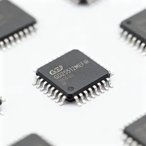
Big Tech’s Race in Advanced Packaging: Cutting-Edge Innovations
As the industry scales up, global semiconductor giants such as TSMC, Samsung, ASE, JCET, and Amkor are fiercely competing in advanced packaging technologies.
1. TSMC: Leading the CoWoS and 3D Packaging Market
TSMC's Chip-on-Wafer-on-Substrate (CoWoS) technology remains the gold standard in HPC and AI processor packaging. The company has doubled CoWoS capacity to meet surging demand from NVIDIA's GB200 AI accelerators.
In addition, TSMC’s 3D SoIC (System on Integrated Chips) platform is set for mass production, further solidifying its leadership in 2.5D and 3D integration technologies.
2. Samsung Expands HBM Packaging and 3.3D Integration
Samsung is investing in next-generation HBM and panel-level packaging (PLP) solutions. The company’s Advanced Packaging Lab in Yokohama is spearheading HBM, AI, and 5G research.
Samsung has also unveiled 3.3D packaging technology, aimed at reducing cost by 22% compared to silicon interposer-based solutions. The company plans to mass-produce this technology by Q2 2026.
3. ASE Advances Chiplet Interconnect Technologies
ASE has developed next-generation microbump interconnect technology, enhancing Chiplet-based semiconductor packaging. The new solution reduces interconnect pitch, improving efficiency for AI and HPC applications.
ASE has also expanded its advanced packaging production sites in Japan, Mexico, and Malaysia to support future demand.
4. JCET: Scaling XDFOI Advanced Packaging
JCET has achieved stable mass production of its XDFOI Chiplet packaging platform, supporting 2D, 2.5D, and 3D integration for AI, HPC, and 5G applications.
JCET is also developing large-area 2D+ packaging solutions and three-dimensional stacking to support next-generation computing demands.
5. Tongfu Microelectronics Invests in High-Density Packaging
Tongfu Microelectronics, a key supplier to AMD, is doubling down on large-size Chiplet packaging. The company has developed Cornerfill and Chip-to-Package Bonding (CPB) technologies, improving chip reliability.
Additionally, Tongfu is exploring glass interposer-based FCBGA packaging for AI, optical communication, and consumer electronics applications.
6. Huatech Technology Expands Automotive Semiconductor Packaging
Huatech is investing $7 billion in a new automotive semiconductor packaging facility, targeting next-gen QFP, Fan-Out, and 3D DRAM packaging. The project is expected to increase its production capacity to 10 million QFP chips per day.
The Future of Advanced Packaging: Opportunities and Challenges
Market Growth Trends
According to TrendForce, the global 2.5D/3D semiconductor packaging market is projected to double in size by 2030, driven by demand for AI, HPC, and data center applications.
Emerging technologies such as Fan-Out Panel-Level Packaging (FOPLP) are also gaining traction, providing cost-effective, high-performance alternatives to traditional packaging methods.
Key Challenges
Despite its rapid expansion, advanced packaging faces major technical and economic hurdles:
High manufacturing costs: The process integration and tooling expenses remain a challenge.
Interconnect density constraints: Achieving high-bandwidth, low-latency interconnections is increasingly difficult.
Yield optimization: 3D stacking increases the risk of defects, requiring advanced quality control measures.
Final Thoughts
As semiconductor complexity continues to rise, advanced packaging is poised to become the industry’s next frontier. Companies that successfully innovate in high-density integration, Chiplet-based solutions, and cost-efficient manufacturing will shape the future of AI, automotive, and high-performance computing markets.