
rf module
Allocation-sensitive sourcing for OEM buyers: what to inspect and what to ask on RFQ. Confirm current terms with the supplier — no invented lead times.
RF Module Decisions: Matching Performance, Sourcing, and Integration Realities
Wireless connectivity has moved from a product differentiator to a baseline expectation, and that shift is compressing design cycles like never before. For engineering teams and procurement buyers, the decision to adopt an RF module—or stick with a discrete design—is now as much a supply-chain and integration calculation as it is an RF performance trade. Doing it well means balancing certified RF performance, allocation-sensitive component availability, and real-world assembly constraints. This article walks through the engineering and sourcing realities that shape that choice, offering a framework that helps you make decisions grounded in datasheet physics, not marketing bullet points.
Why RF Modules Are Compressing Design Cycles—and What It Costs
Pre-certified RF modules fundamentally change the time-to-market equation. Instead of spending months tuning a discrete transceiver front‑end, navigating multi‑region regulatory approvals, and iterating PCB layouts for controlled‑impedance traces, you drop in a module that already carries FCC, ISED, and CE marks. Recent analysis from EE Times underscores how IoT connectivity acceleration is pushing product teams toward module‑based architectures, particularly in industrial sensor, smart home, and edge‑AI devices where wireless performance isn’t the product’s core IP—it’s just a must‑have feature.
That compression comes at a cost, both per‑unit and strategically. Modules carry a BOM premium over a bare metal transceiver IC plus passives, but the full cost picture must account for the engineering hours saved, the reduced certification cycle (often 8–12 weeks eliminated), and the lower risk of an RF re‑spin. The real friction, however, is supply volatility. The post‑pandemic component landscape has magnified the make‑vs‑buy decision because key RF chipsets—particularly those for Wi‑Fi, Bluetooth LE, and multi‑protocol sub‑GHz bands—are often fabricated on process nodes that compete for capacity with automotive and industrial MCUs. This makes many popular module families allocation‑sensitive. For procurement, that means you treat RF module supply as a risk that must be verified via RFQ, not assumed from a distributor’s inventory dashboard.
Buyers who treat a module as a guaranteed, off‑the‑shelf C.O.T.S. item can be blindsided. The underlying transceiver die or power amplifier may be on allocation while the module vendor still quotes “standard” lead times. Always confirm allocation‑backed lead time with the supplier, request visibility into the chipset fab loading whenever possible, and have a conversation about second‑source qualification early in the design phase. The cost of a module approach isn’t just the component price; it’s the fragility of a single‑sourced, opaque supply chain if you haven’t done the homework upfront.
Key Takeaway: RF modules collapse development risk but concentrate supply risk. The value proposition holds only when you treat sourcing as an active, allocation‑aware process, not a one‑time part number assignment.
What’s Inside an RF Module: The Core Signal Chain and Key Specs
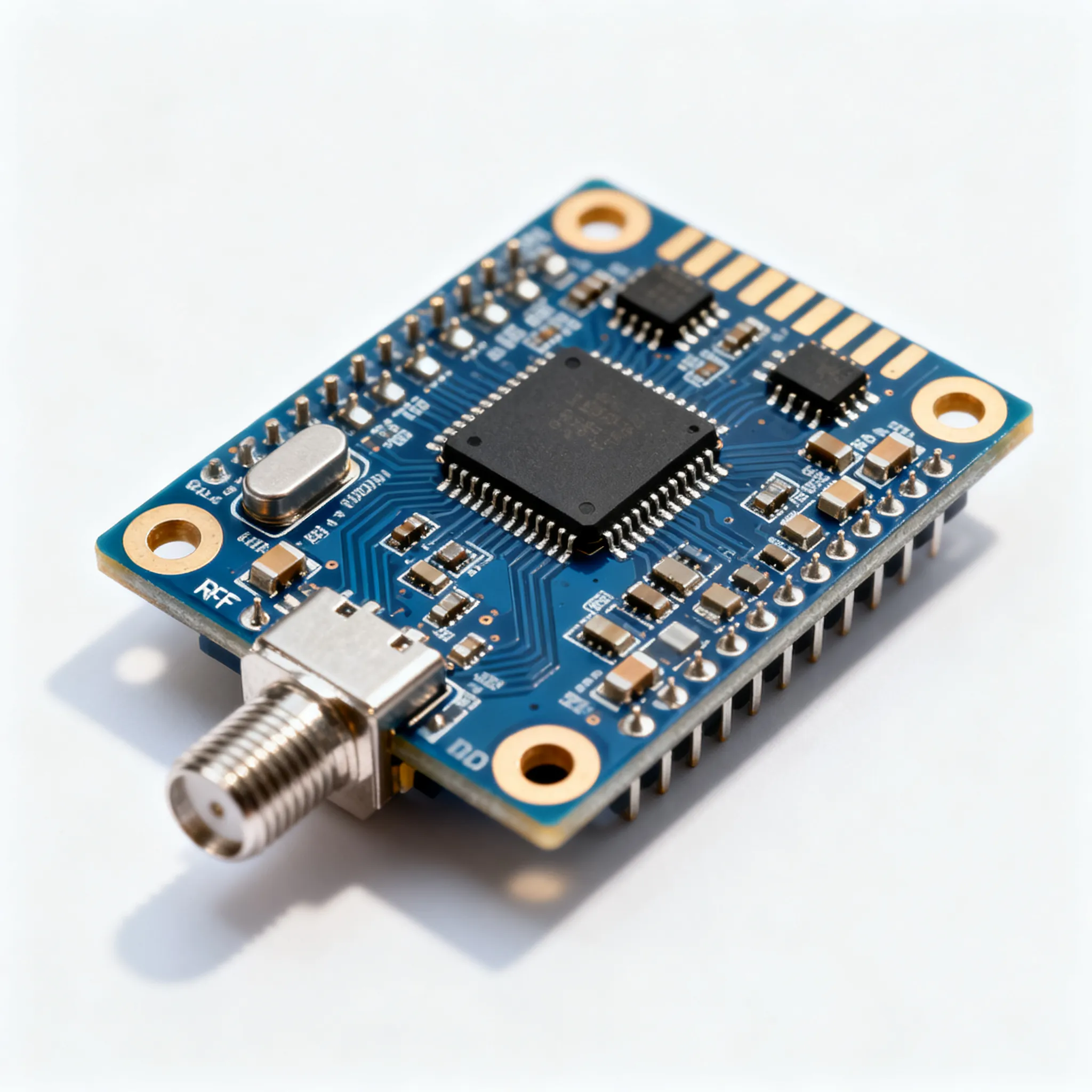
An RF module packages a complete wireless node—transceiver or System‑on‑Chip (SoC), power amplifier (PA), low‑noise amplifier (LNA), antenna matching network, and often a built‑in antenna or U.FL connector—on a small, shielded PCB. The integration simplifies layout to a few power‑supply, digital I/O, and ground connections, but it also shifts responsibility for critical RF parameters to the module vendor. Understanding what those parameters mean, and how they are specified, is the difference between a design that works on the first prototype and one that fails in the field.
The core signal chain determines the link budget: the arithmetic sum of output power, antenna/connector losses, and receiver sensitivity that defines the maximum path loss sustainable for a given data rate. Output power is often quoted at the chip pad, not at the module’s antenna port—a subtlety that can cost you 2–4 dB if you don’t read the fine print. Sensitivity is equally context‑dependent, varying with modulation scheme, data rate, and packet error rate (PER) target. Modules also carry spurious emission limits, current consumption profiles across TX/RX/sleep states, and often integrated DC‑DC converters that affect power‑supply ripple requirements. These numbers must be evaluated over the full temperature and voltage window, because sensitivity and output power can drift several dB at the extremes.
Equally important is the physical layout discipline that the module imposes. While the module itself is a self‑contained RF island, the PCB that hosts it must still follow controlled‑impedance rules for the antenna feed, maintain sufficient ground‑plane continuity, and respect keep‑out zones. Guidance from IPC Standards, particularly IPC‑2221 for controlled‑impedance design, remains essential for integrating any module into a system that must pass radiated emissions and immunity testing. The table below compares typical integration levels and the associated performance parameters you’ll need to weigh.
| Integration Level | Representative Architecture | Key Performance Parameters (Module‑Level) | Typical Application Constraints |
|---|---|---|---|
| Bare transceiver SoC (module with external antenna) | Nordic nRF52/nRF53, TI CC26xx, ST STM32WL in third‑party module with U.FL pad | Output power at antenna port, sensitivity at BER=0.1%, spurious at max power, harmonic compliance | Requires external antenna, matching verification; gives most placement flexibility but demands controlled‑impedance layout |
| Module with integrated chip antenna | Espressif ESP32‑WROOM, Murata Type 1DX, u‑blox NINA‑B4 with PCB trace antenna | Total radiated power, radiation efficiency, impedance bandwidth, desense sensitivity in typical enclosure | PCB keep‑out zones critical; de‑tuning near metal or battery can cut range by 50% or more |
| Module with integrated ceramic antenna | u‑blox SARA‑R5 (LTE‑M/NB‑IoT), Telit ME910 with integrated chip antenna variant | Return loss in free space, efficiency vs. ground‑plane size, peak gain | Compact but narrow bandwidth; often requires additional pi‑network for matching if enclosure shifts resonance |
| Module with RF connector (U.FL/IPEX) | Multi‑radio Wi‑Fi/BT modules (Murata 1MW, TI WL18xx modules) | Conducted output power, connector insertion loss (0.3–0.8 dB), sensitivity at connector pin | Antenna design and cable assembly passed to the product team; most flexible for industrial enclosures |
The table highlights a central truth: a module’s declared performance is only as useful as your ability to replicate its characterization conditions. When a datasheet shows +20 dBm output power at 1 Mbps BLE, you need to confirm whether that measurement is taken at the chip output (before the matching network and antenna switch) or at the module’s RF pin. A module that claims -98 dBm sensitivity at the connector may deliver -95 dBm once you account for board‑level insertion loss and enclosure detuning. Never accept a single headline number without these details.
Module vs. Discrete RF Design: Integration Gains and Flexibility Trade‑Offs
Choosing between a module and a discrete RF design is not a simple BOM cost comparison. It’s a multi‑dimensional trade that touches schedule, certification, supply‑chain resilience, and the performance headroom you can extract. A discrete design built around a transceiver IC like Nordic’s nRF52840, ST’s STM32WL, or TI’s CC2652R, combined with a discrete PA/LNA, balun, and passives, gives you complete control over the antenna match and the freedom to optimize the link budget for your specific enclosure. But that control demands deep RF expertise, longer development, and—crucially—dedicated certification efforts for each target geography.
A module encapsulates that expertise and absorbs the certification burden. You lose the ability to fine‑tune the matching network (the module vendor has already locked it), but you gain a known‑good RF front‑end that will pass regulatory radiated tests without iteration—provided you don’t violate the modular grant conditions by changing the antenna type, extending the trace, or re‑chipping the module’s output power. The supply‑chain implications are equally nuanced. A discrete BOM spreads risk across a transceiver available from multiple distributors, standard passives, and a commodity crystal. A module, however, may be single‑source, tied to one module vendor who in turn depends on a sole‑source chipset. When that chipset hits allocation, the entire module line is vulnerable.
The comparison matrix below frames the decision points in terms an engineering‑procurement pair can discuss jointly.
| Comparison Metric | Module‑Based Solution (e.g., u‑blox NINA‑B4, Murata 1DX) | Discrete RF Design (e.g., Nordic nRF52840 + discrete passives) | Selection Criteria & Failure Boundary |
|---|---|---|---|
| Bill‑of‑material (BOM) line items | 1 module + some decoupling caps; typically <10 additional passives | 1 transceiver IC + 20–35 passives, crystal, balun, antenna matching network | BOM complexity directly impacts procurement workload and assembly yield; module wins for rapid prototyping and lower‑volume production |
| Time‑to‑certification | Pre‑certified modular approval (FCC/CE); end‑product verification only | Full intentional radiator testing for each region; expect 6–14 weeks plus design‑debug iterations | If product launch window is <6 months and RF is not core IP, module is strongly favored |
| RF performance headroom | Factory‑tuned matching, but cannot be re‑optimized for a specific enclosure; typically 2‑4 dB loss vs. theoretical optimum | Can tune matching for exact antenna and enclosure; achievable sensitivity may be 3‑5 dB better | For battery‑powered sensors where every dB extends range, discrete gives measurable edge—but only if RF team is experienced |
| Supply‑chain single‑source risk | Module often sole‑source; verify single‑source risk via manufacturer / distributor documentation | Transceiver IC may be multi‑sourced or second‑sourceable via pin‑compatible alternatives (evaluate candidates like GD32/APM32 if applicable) | Products with 5‑year lifecycles must factor in discontinuation risk; module obsolescence can force a complete re‑design |
| PCB area & layout effort | Compact, shielded footprint; minimal RF layout beyond antenna feed | Requires controlled‑impedance traces, ground stitching, supply filtering; adds 15‑25% more area for matching network | Space‑constrained wearables benefit from module, but high‑volume cost‑sensitive products may accept layout effort for unit cost savings |
| Re‑design agility (e.g., changing radio protocol) | Locked to module firmware and supported protocols; swapping module may require new footprint | SoC‑based designs can potentially adapt firmware for new standards if the RF front‑end bandwidth allows | If multi‑protocol flexibility is critical, verify that the module stack supports future protocols without a hardware change |
In practice, the decision often splits along production volume and engineering capability. Low‑ to mid‑volume products (hundreds to a few thousand units) that must ship quickly lean heavily toward modules. High‑volume consumer products where every penny of BOM cost is scrutinized and RF design skill is in‑house can justify the discrete route—provided the supply of the core transceiver remains secure. Both paths require a clear understanding of the allocation risk. A module that appears to solve all RF problems becomes a liability if its lead‑time suddenly extends because its chipset vendor has prioritized automotive customers. Confirm allocation‑backed lead time with the supplier and maintain a qualified alternative layout if volume deployments are planned.
Sourcing and Specifying RF Modules Without Over‑Engineering
Specifying an RF module shouldn’t become an exercise in chasing datasheet maxima. The most effective approach is to identify the minimum viable RF performance your product actually needs and then to verify that the module can deliver that performance under worst‑case manufacturing and environmental conditions. That means digging into datasheet caveats, validating the RF matching over temperature, and aligning the module’s lifecycle with your product’s expected lifetime. For assembly reliability, IPC Standards such as IPC‑A‑610 provide acceptance criteria for the soldering of module castellations and LGA pads that directly affect long‑term RF ground continuity.
The sourcing checklist below breaks down the verification steps that bridge the gap between a confident paper specification and a reliable production launch.
| Verification Parameter | What to Confirm (Request from Supplier) | Risk if Overlooked | Recommended Validation Method |
|---|---|---|---|
| Output power reference plane | Datasheet value at antenna port (after internal matching, switch, and connector) | Under‑estimated link budget by 2‑4 dB; range may be cut by 30% | Conducted power measurement on first‑article samples at module RF pin |
| Sensitivity vs. temperature & voltage | Production‑test sensitivity over -40 to +85 °C at nominal and minimum VCC, with same packet configuration as your application | Cold‑car startup or battery brown‑out conditions can cause unexpected link drops | Swept‑temperature test in thermal chamber with PER monitoring |
| Harmonic compliance at max power | Module‑level radiated or conducted harmonic levels meet the target regional limits with the final antenna and enclosure | Pre‑certified module grant may be invalidated by altered antenna or enclosure; re‑testing required | Radiated spurious survey in product enclosure with compliance partner |
| Module lifecycle commitment | Vendor’s EOL policy and minimum production span; confirm via RFQ | Product may require a redesign in 3–5 years despite module being “active” | Request product change notification (PCN) agreement and check for planned EOL notices |
| Batch‑to‑batch RF matching consistency | Test data reports for key parameters (output power, current consumption, return loss) from at least 3 batches | Unit‑to‑unit variation can cause marginal links to fail in the field | Side‑by‑side OTA test of multiple samples in target enclosure |
| Soldering profile and reflow capability | Module’s recommended reflow profile vs. your assembly line’s capability; moisture sensitivity level (MSL) | Cracked ceramic antennas or lifted castellations leading to intermittent RF performance | Cross‑section inspection per IPC‑A‑610 Class 2/3 acceptance; request module’s wetting‑balance report |
Smart procurement teams use these verification points not just as a one‑time qualification gate but as a continuous monitoring framework. For RF modules that are allocation‑sensitive, demand that your supplier provide visibility into the underlying chipset lead‑time and any upcoming fab transitions. A module that meets all performance metrics on day one can become a line‑down risk if the chipset inside moves to a smaller geometry node and the module vendor must re‑qualify—a process that can interrupt supply for months. Negotiate safety‑stock buffers tied to your forecast, and, if the product volume justifies it, fund the qualification of a second module layout that uses a different chipset vendor. The cost of a duplicate layout is often far less than the opportunity cost of a stalled production line.
RF Module FAQ: Engineering and Procurement Questions That Shape BOM Decisions
Q: How do I confirm that a module’s output power and sensitivity will satisfy my link budget over full temperature and voltage range?
Cross‑check datasheet conditions—particularly output power at the antenna port vs. chip level, sensitivity at the module pin, and derating curves. Request production‑test data and evaluate margin for PCB insertion loss, enclosure attenuation, and antenna mismatch. For critical links, plan a swept‑power debug stage in the prototype phase to verify real‑world range margins. Don’t assume the room‑temperature numbers hold at -40 °C or when the battery is near cut‑off; a 3 dB drop can halve the effective range.
Q: When does an RF module’s integrated antenna save BOM cost and when does it force expensive redesign?
Integrated antennas reduce component count and tuning effort for compact, plastic‑enclosed devices but severely limit placement and grounding options. Evaluate radiation efficiency and impedance bandwidth against your product’s mechanical constraints early; a self‑contained antenna module often demands larger keep‑out zones and can de‑tune near metal. For metal enclosures or high‑gain requirements, an external antenna with a certified connector may be cheaper overall, and you avoid the hidden cost of a re‑design when the integrated antenna fails to meet range in the real product.
Q: Are module pre‑certifications (FCC, CE) globally reusable, or will I still need national testing?
Pre‑certified modules simplify testing under modular approval rules, but exact conditions vary. Re‑use is valid only if the end‑product’s antenna type, trace length, and power level match the certification’s grant conditions. For regions like Japan, Korea, or Brazil, additional filings may be required despite a US/EU modular approval. Always confirm with a compliance partner, not just the module vendor’s claim. A module vendor’s declaration of “FCC compliant” does not automatically grant your end‑product the same status; the module must be used exactly as certified.
Q: What lead‑time risks should I anticipate with popular sub‑GHz and Wi‑Fi modules, and how can I buffer?
Module lead times can spike when core chipset shortages occur; single‑source modules tied to a specific chipmaker are especially vulnerable. Cross‑qualify a pin‑compatible alternative early in development, negotiate safety‑stock agreements with distributors, and monitor chipset fab loading reports. For high‑volume products, a double‑source strategy—even at the cost of a second PCB layout—can prevent line‑down events. Do not rely on a module vendor’s generic “ample stock” claim; treat supply as allocation‑sensitive and confirm allocation‑backed lead time with the supplier.
Q: How do I compare module performance claims fairly when vendors measure sensitivity and output power differently?
Normalize all numbers to the antenna port or connector at a standard BER/PER, and note whether the published value includes or excludes internal matching losses. For output power, compare at the same harmonic compliance level and modulation mode. For sensitivity, check the same data rate and coding scheme. Request per‑batch test reports and, for critical decisions, perform a side‑by‑side over‑the‑air test in your target enclosure rather than relying on data‑sheet alone. A module that looks 2 dB better on paper may, in practice, suffer worse detuning in your enclosure.
Q: How can I verify the real operating range of a module before committing to production volumes?
Perform a physically representative range test with several modules, using statistical sampling to capture unit‑to‑unit variation. Measure packet error rate at multiple distances in the intended environment (including obstacles and interference). Correlate the results with link budget predictions to identify hidden issues like poor antenna detuning, PLL phase noise, or board‑level interference. Document a threshold margin that accounts for aging and environment. A link that works at 10 meters in the lab may fail at 8 meters in a metallic enclosure after six months of temperature cycling; building that margin into your specification is a cheap insurance policy.
References & Further Reading
- EE Times — Electronics Engineering News: Analysis of IoT connectivity and wireless design trends.
- IPC — Association Connecting Electronics Industries: Standards for controlled‑impedance design (IPC‑2221) and soldering acceptance (IPC‑A‑610).
- Nordic Semiconductor — nRF52840 SoC: Reference for discrete transceiver and module‑embedded solution evaluation.
- Texas Instruments — CC2652R: Multi‑protocol wireless MCU frequently used in both module and discrete designs.
- STMicroelectronics — STM32WL Series: Sub‑GHz and LoRa‑capable wireless SoC for module and chip‑down approaches.
- Espressif — ESP32 SoC: Widely adopted in modules; example of single‑chip Wi‑Fi/BT integration.
- u‑blox — NINA‑B4 Series: Representative stand‑alone Bluetooth 5.1 module for evaluation as a drop‑in candidate.
- Murata — Connectivity Modules: Broad portfolio of pre‑certified Wi‑Fi/BT/LTE modules; useful for comparing integration levels.
- IC-Online: Multi‑supplier platform for RFQ, BOM upload, and sourcing allocation‑sensitive components.
Every project that depends on wireless connectivity eventually faces the tension between performance, schedule, and supply certainty. RF modules can shift that equation dramatically in your favor—shortening development, reducing certification cost, and delivering a known‑good RF front‑end. But they transfer the supply‑chain burden from a diverse BOM to a concentrated, often single‑source component. Treat module selection as an active, sourcing‑conscious decision rather than a passive component pick. Validate critical specs against your specific enclosure and environment, confirm allocation‑backed lead times, and maintain a second‑source path even when the module promises to be the simplest route. The module market is dynamic, and a sourcing strategy built on transparency and verification will protect your production schedules better than any datasheet promise.
Next Step: For allocation‑sensitive RF modules and mixed‑BOM requirements, request a quote or upload your BOM via IC-Online. Our platform connects you with verified distributors to help you secure supply without relying on speculative inventory claims.