Aiwei Photonics Headquarters Base Structure Fully Topped Out
Recently, the Aiwei Photonics Headquarters Base project, which is listed as a key project by both Guangdong Province and Guangzhou City, has completed the topping out of its main structure.
Recently, the Aiwei Photonics Headquarters Base project, which is listed as a key project by both Guangdong Province and Guangzhou City, has completed the topping out of its main structure.
According to project officials, following the topping out, the project will officially enter the decoration and electromechanical installation phase, with the entire project expected to be completed by June next year.
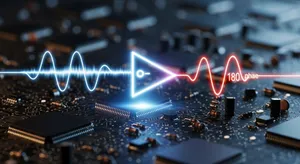
Aiwei Technology’s official WeChat account stated that the Aiwei Photonics SABAR® 5G surface acoustic wave (SAW) filter chip R&D and production headquarters is located in the China-Singapore Guangzhou Knowledge City in Huangpu District. The project covers a total building area of approximately 150,000 square meters. It will include production and R&D facilities, including factories, research workshops, and warehouses, while adopting internet thinking and Industry 4.0 principles. The aim is to create a modern industrial park that promotes R&D innovation, collaboration, and green, sustainable development.

Once operational, Aiwei Photonics will scale up production of its proprietary SABAR® 5G SAW filter chips and modules, with an estimated annual production capacity of 3 billion SABAR® 5G SAW filter chips. This will significantly boost the market share and influence of China’s domestically developed 5G SAW filter chips and modules.