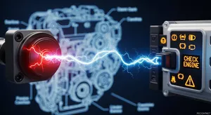
ASML and Imec Expand Strategic Partnership to Advance Semiconductor Innovation
ASML, the world’s leading semiconductor equipment manufacturer, has announced a new five-year strategic partnership with Imec, Belgium’s premier microelectronics research center. This collaboration aims to drive cutting-edge innovations in semiconductor manufacturing, focusing on next-generation lithography, memory solutions, and advanced packaging technologies.
Five-year collaboration focuses on next-generation semiconductor technologies
Key areas include high-NA EUV, silicon photonics, memory, and advanced packaging
ASML's latest lithography systems to be integrated into research projects
ASML, the world’s leading semiconductor equipment manufacturer, has announced a new five-year strategic partnership with Imec, Belgium’s premier microelectronics research center. This collaboration aims to drive cutting-edge innovations in semiconductor manufacturing, focusing on next-generation lithography, memory solutions, and advanced packaging technologies.
Expanding ASML-Imec Collaboration
This agreement builds on the long-standing partnership between ASML and Imec. Their latest collaboration will integrate ASML’s full product portfolio, including:
- High-NA EUV lithography (0.55 NA) – Enabling smaller, faster, and more efficient chips
- Standard EUV lithography (0.33 NA) – Enhancing extreme ultraviolet manufacturing
- DUV immersion lithography – Supporting mature and cost-effective semiconductor nodes
- YieldStar optical metrology and HMI multi-beam technology – Improving precision and defect detection

Key Focus Areas: Memory, Silicon Photonics, and Advanced Packaging
The new partnership aims to develop next-generation semiconductor solutions in key areas:
- Memory Innovation – Improving DRAM, NAND, and emerging storage solutions for AI and high-performance computing (HPC).
- Silicon Photonics – Enhancing data transmission speeds for next-gen computing and networking applications.
- Advanced Packaging – Developing innovative chiplet integration and 3D stacking technologies to optimize performance and power efficiency.
ASML’s Commitment to High-NA EUV
ASML and Imec previously announced plans to establish a dedicated High-NA EUV lithography lab in Veldhoven, Netherlands. High-NA EUV, a breakthrough in extreme ultraviolet (EUV) lithography, is expected to increase resolution by 60% compared to earlier EUV generations, enabling the production of smaller, faster, and more efficient chips.
ASML anticipates that customers will begin using High-NA EUV technology for commercial chip production by 2025-2026, marking a major milestone in semiconductor fabrication.
Shaping the Future of Semiconductor Manufacturing
By combining ASML’s industry-leading lithography expertise with Imec’s cutting-edge semiconductor research, this partnership will accelerate the development of scalable, sustainable, and high-performance semiconductor solutions.
As AI, 5G, and quantum computing drive demand for more powerful and energy-efficient chips, ASML and Imec’s collaborative innovations will play a critical role in shaping the future of the global semiconductor industry.