The Global Semiconductor Equipment Race Intensifies
Driven by advancements in AI, IoT, 5G, and autonomous driving, the global demand for semiconductor equipment continues to grow, particularly in high-end chip manufacturing and advanced packaging. In response, multiple countries have ramped up investments to maintain competitiveness in the global semiconductor value chain. Notably, recent developments from China and Russia highlight their respective efforts to strengthen domestic capabilities in this critical industry.
Driven by advancements in AI, IoT, 5G, and autonomous driving, the global demand for semiconductor equipment continues to grow, particularly in high-end chip manufacturing and advanced packaging. In response, multiple countries have ramped up investments to maintain competitiveness in the global semiconductor value chain. Notably, recent developments from China and Russia highlight their respective efforts to strengthen domestic capabilities in this critical industry.
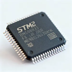
China’s Semiconductor Equipment Industry on the Rise
Global leaders in semiconductor equipment production are concentrated in the U.S., the Netherlands, Japan, and South Korea, dominating areas like lithography, etching, and deposition. However, China has made significant strides, leveraging increased R&D investments and localization efforts to carve out a growing share in etching, CVD, PVD, and testing equipment.
Notable Chinese Semiconductor Equipment Companies
-
Beijing NAURA Technology Group
Known for platform-based solutions, NAURA offers advanced tools such as etching machines, PVD, CVD, ALD, and cleaning systems. As of mid-2024, its industrialization and R&D expansion projects reported progress rates of 59.65%, 86.63%, and 72.7%, respectively. -
AMEC (Advanced Micro-Fabrication Equipment Inc.)
Specializes in plasma etching tools and TSV equipment for advanced packaging. AMEC continues to expand its product lineup based on customer needs. -
Hwatsing Technology
Focused on CMP (Chemical Mechanical Polishing) systems, Hwatsing's new polishing machines and wafer thinning tools have gained traction among leading customers. -
Shanghai Shengmei Semiconductor
Competes with top-tier global suppliers in wafer cleaning and electroplating equipment. Its PECVD and track systems are under validation, with 50% process coverage expected by late 2024. -
Recent Innovations in China
- Yanwei Semiconductor delivered its first 300mm Atomic Layer Deposition (ALD) equipment to a top domestic client.
- China Semiconductor Photonics secured orders for 8-inch SiC defect inspection tools, addressing high-precision requirements for SiC wafer manufacturing.
- Guangzhou Yuesheng Semiconductor announced large-scale shipments of optimized SiC epitaxy equipment.
Warning Signals for China’s Semiconductor Equipment Market
Despite the rapid growth, challenges loom. According to SEMI, China’s semiconductor equipment spending is projected to hit $40 billion in 2024, but demand may decline in 2025 as production lines stabilize. This reflects a cyclical adjustment rather than a long-term contraction. With continued advancements and localization, demand for equipment in AI, 5G, and automotive electronics will likely sustain growth over the long term.
Russia’s Push for Domestic Semiconductor Equipment
Russia has also accelerated its efforts to develop domestic semiconductor manufacturing tools. Supported by the Ministry of Industry and Trade, Russia is focusing on 200mm wafer production tools for 180nm to 90nm nodes. Backed by a ₽17 billion ($17.7 million) grant, these developments aim to reduce reliance on foreign equipment.
Russian Semiconductor Equipment Milestones
- Short-term Goals: By 2026, Russia aims to produce equipment for single-crystal growth, wafer cutting, polishing, and defect control, along with 130nm photolithography tools.
- Long-term Goals: By 2030, the country targets 65nm and 90nm lithography systems, narrowing its technological gap with global leaders.
Despite progress, Russian equipment remains significantly behind, lagging by 25-28 years compared to leading-edge manufacturing.

Semiconductor Equipment Landscape: Key Technologies
Semiconductor equipment falls into two main categories: front-end (wafer manufacturing) and back-end (packaging and testing). Front-end processes, including lithography, etching, deposition, and ion implantation, dominate the market, accounting for 81% of global equipment demand.
Core Equipment in Semiconductor Manufacturing
- Lithography: The most complex and expensive semiconductor tool, critical for advanced nodes. EUV and immersion lithography dominate the market.
- Etching: Led by plasma dry etching for high-precision patterning.
- Deposition: Includes PVD and CVD methods for creating thin films essential for modern chips.
Opportunities and Challenges Ahead
The global semiconductor equipment market remains on a growth trajectory, driven by advanced nodes, AI, and new applications in 5G and automotive electronics. However, increased competition, geopolitical tensions, and supply chain disruptions pose challenges. As countries like China and Russia intensify their efforts, the semiconductor industry stands at the crossroads of innovation and transformation.