Intel Begins Production with ASML's High-NA EUV Machines, Doubling Reliability
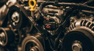
Intel has officially launched production using the first two High-NA Extreme Ultraviolet (EUV) lithography machines from ASML, marking a significant step forward in semiconductor manufacturing technology. Early results indicate that these cutting-edge machines are already outperforming previous models in terms of reliability, potentially reshaping Intel’s competitive edge in chip fabrication.
Intel has officially launched production using the first two High-NA Extreme Ultraviolet (EUV) lithography machines from ASML, marking a significant step forward in semiconductor manufacturing technology. Early results indicate that these cutting-edge machines are already outperforming previous models in terms of reliability, potentially reshaping Intel’s competitive edge in chip fabrication.
High-NA EUV Machines: A Game-Changer for Intel
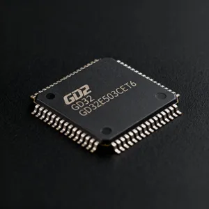
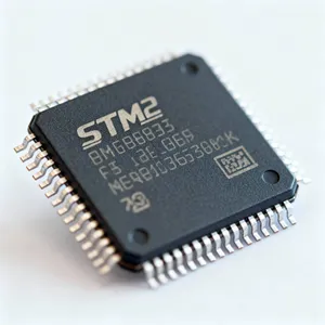
According to Steve Carson, Senior Principal Engineer at Intel, the company has already processed 30,000 wafers using ASML’s advanced High-NA EUV machines within just one quarter. Each wafer contains thousands of high-performance computing chips, highlighting the scalability and efficiency of the new technology.
This move reflects a strategic pivot for Intel, which aims to regain its competitive advantage after falling behind rivals like TSMC when it struggled with the rollout of earlier-generation EUV machines. It took Intel nearly seven years to fully integrate the previous generation of EUV technology, allowing competitors to surge ahead.
Improved Reliability and Efficiency
Early testing of ASML’s High-NA EUV machines has shown promising results. Carson revealed that these new machines are twice as reliable as their predecessors. This improved reliability means Intel can maintain a consistent wafer output rate, which is critical for scaling production efficiently.
One of the biggest advantages of High-NA EUV technology is its ability to print finer circuit patterns with fewer exposure passes. The new machines can complete tasks that previously required multiple steps with a single exposure and a handful of processing stages. Specifically, Carson highlighted that:

High-NA EUV machines need just one exposure and a single-digit number of processing steps.
The previous generation required three exposures and around 40 processing steps for the same workload.
This improvement not only saves time but also significantly reduces manufacturing costs.
Powering Intel’s 18A and Future 14A Process Technologies
Intel plans to utilize the new High-NA EUV machines in the development of its advanced 18A process node. This technology, which promises a 30% increase in chip density and a 15% improvement in power efficiency per watt compared to previous nodes, is expected to enter mass production later this year for new PC processors.
Looking ahead, Intel also plans to fully integrate High-NA EUV machines into its upcoming 14A process. Although the company has yet to announce a specific timeline for 14A mass production, the successful implementation of High-NA EUV technology will be key to maintaining Intel’s competitive edge in the global semiconductor market.
Why This Matters for the Semiconductor Industry
ASML’s High-NA EUV technology represents a major advancement in semiconductor manufacturing, offering faster, more efficient, and cost-effective chip production. For Intel, successfully deploying these machines could be a turning point in its race against leading foundries like TSMC and Samsung.
By reducing the number of exposure cycles and streamlining production steps, Intel is positioning itself to reclaim its leadership position in chip innovation and manufacturing.