Decoding T Flip Flops for Aspiring Engineers
A T flip-flop is a fundamental digital logic circuit. This specific flip-flop is a type of bistable multivibrator

A T flip-flop is a fundamental digital logic circuit. This specific flip-flop is a type of bistable multivibrator designed for 1-bit data storage. The "T" in T flip flop stands for Toggle. This toggle flip flop has a unique working principle where its output flips to the opposite of its current state. This simple toggling action is vital across digital electronics. The main applications for the t flip flop stem from this core behavior.
Note: The T flip flop circuit is a bi-stable device. This means the flip-flop has two stable states, making it an essential memory element in many digital systems. We will explore the t flip-flops and t flip flops in detail.
Key Takeaways
- A T flip-flop is a basic digital circuit. It stores one bit of data. The 'T' means 'Toggle'.
- The T flip-flop has two main actions. It can 'Hold' its current state or 'Toggle' to the opposite state.
- You can build a T flip-flop from other flip-flops. Using a JK flip-flop is the easiest way.
- T flip-flops are useful for two things. They divide frequencies and build binary counters.
- Understanding T flip-flops helps you design digital systems. This includes things like timers and clocks.
Understanding the T Flip-Flop Core Function
To truly grasp the power of the t flip flop, we must first understand its fundamental logic. The behavior of this bi-stable device is predictable and defined by a simple set of rules. The working of t flip flop is governed by its single 'T' input and its current state. Let's break down this core function into its two main components: the truth table and the characteristic equation.
The Truth Table: Hold vs. Toggle
A truth table is a map that shows how a logic circuit will behave based on all possible inputs. For a t flip-flop, the inputs are the 'T' signal and the flip-flop's current output state, which we call Q. The output is the next state, Q_next.
The t flip flop truth table is refreshingly simple. It demonstrates the two modes of operation:
| T Input | Current State (Q) | Next State (Q_next) | Mode |
|---|---|---|---|
| 0 | 0 | 0 | Hold |
| 0 | 1 | 1 | Hold |
| 1 | 0 | 1 | Toggle |
| 1 | 1 | 0 | Toggle |
Let's examine these two modes:
- Hold State (T = 0): When the T input is low (0), the flip-flop ignores the clock pulse. The output
Q_nextremains the same as the current outputQ. The flip-flop "holds" its current value, acting as a basic memory cell. - Toggle State (T = 1): When the T input is high (1), the t flip-flop becomes active. On the next clock edge, the output
Q_nextflips to the complement of its current stateQ. IfQis 0, it becomes 1. IfQis 1, it becomes 0. This is the "toggle" action that gives the t flip flop its name.
For Advanced Design: The Excitation Table While a truth table predicts the next state from a given input, an excitation table does the reverse. It tells you what input (
T) is needed to transition from a present state (Q) to a desired next state (Q_next). This is crucial for designing sequential circuits.
Present State (Q) Next State (Q_next) Required Input (T) 0 0 0 0 1 1 1 0 1 1 1 0
The Characteristic Equation
The characteristic equation is the algebraic expression that mathematically describes the t flip flop working principle. It provides a concise formula for the logic shown in the truth table.
The characteristic equation for the t flip-flop is:
Q_next = T ⊕ Q
Here, the ⊕ symbol represents the Exclusive OR (XOR) logic operation. The XOR gate outputs a 1 only when its two inputs are different. This perfectly defines the toggle behavior:
- If T = 0 (Hold):
Q_next = 0 ⊕ Q. The result is equal toQ. The state does not change. - If T = 1 (Toggle):
Q_next = 1 ⊕ Q. The result is equal toQ'(the inverse of Q). The state flips.
This elegant equation Q_next = TQ' + T'Q is derived from a Karnaugh map of the truth table, confirming that the XOR logic is the mathematical heart of the t flip-flop. This equation is fundamental for analyzing and designing digital circuits with t flip flops.
A Note on Real-World Performance: Propagation Delay ⏱️ The logical working of a flip-flop is instant in theory, but not in reality. Propagation delay is the tiny amount of time it takes for the output (Q) to actually change after the clock edge arrives. This delay is critical because it limits how fast your circuit can run. The maximum clock frequency of a circuit using flip-flops is determined by:
- The clock-to-output delay of the first flip-flop.
- The propagation delay of any logic gates between flip-flops.
- The setup time required by the next flip-flop.
For example, if a flip-flop has an 8 ns propagation delay, a 1 ns setup time, and a 1 ns hold time, the minimum clock period is the sum of these delays (10 ns). This limits the maximum frequency to 1 / 10 ns = 100 MHz. Understanding these timing characteristics is essential for any engineer designing high-speed digital systems.
How to Build a T Flip Flop
In many digital designs, you will not find a dedicated T flip-flop IC (Integrated Circuit). Instead, engineers build them using other common types of flip-flops. This is a practical skill that also deepens your understanding of how these circuits relate to one another. Let's explore the two most common methods for creating a t flip flop.
Deriving from a JK Flip-Flop
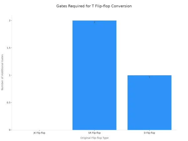
The most straightforward way to create a t flip flop is by modifying a JK flip-flop. This method is highly efficient because it requires no additional logic gates.
The conversion process is simple:
- Take a standard JK flip-flop.
- Connect the
Jinput and theKinput together. - This common connection now serves as the single
Tinput.
This works perfectly because the JK flip-flop's behavior aligns directly with the T flip-flop's requirements.
- When
T = 0(meaningJ=0andK=0), the JK flip-flop is in its "Hold" state. The output does not change. - When
T = 1(meaningJ=1andK=1), the JK flip-flop enters its "Toggle" state. The output flips to its complement.
This inherent ability to toggle makes the JK flip-flop the ideal foundation for a t flip flop circuit. The chart below shows how this conversion compares to others in terms of hardware efficiency.
Converting from a D Flip-Flop
You can also build a t flip-flop from a D (Data) flip-flop. This method clearly demonstrates the logic behind the toggle function. It requires one external component: an Exclusive-OR (XOR) gate.
The logic is based on the characteristic equation we saw earlier. The D input must be fed the result of T ⊕ Q.
- The D input of the flip-flop connects to the output of the XOR gate.
- The inputs to the XOR gate are the external
Tsignal and the flip-flop's own output,Q.
This feedback loop ensures the D flip-flop behaves like one of the t flip flops. The Boolean function for the D input is D = T ⊕ Q(t). This setup creates the necessary logic for the hold and toggle states, as shown in the table below.
| T Input | Present State Q(t) | Next State Q(t+1) | Required D Input |
|---|---|---|---|
| 0 | 0 | 0 | 0 |
| 0 | 1 | 1 | 1 |
| 1 | 0 | 1 | 1 |
| 1 | 1 | 0 | 0 |
Note on Circuit Stability 💡 The feedback loop in this design, where the output
Qis fed back to the input logic, is essential. This feedback introduces a tiny but critical time lag. This delay ensures the circuit has enough time to settle into its new state after a toggle, preventing instability and ensuring reliable operation.
Key Applications for T Flip-Flops
The simple toggle function of the t flip flop is the key to its most important applications in digital electronics. Understanding these uses is crucial for any aspiring engineer. The two primary applications of t flip flop are frequency division and the construction of binary counters. These concepts are not just theoretical; they are the building blocks of complex systems. For instance, companies like Nova Technology Company (HK) Limited, a HiSilicon-designated solutions partner, leverage these fundamental principles. They provide advanced chip-level solutions and system integration where precise timing, generated by frequency dividers, and state tracking, managed by counters, are essential for performance.
Frequency Division with a T Flip-Flop
One of the most powerful applications for a t flip-flop is frequency division. When the T input of a flip-flop is held high (connected to logic '1'), its output toggles for every clock pulse. This means the output waveform has exactly half the frequency of the input clock signal.
- Input Clock: Has a frequency
f. - Output Q: Toggles once for every two clock pulses, resulting in a frequency of
f/2.
This makes a single t flip flop an effective divide-by-2 circuit.
How do we divide by more? ⚙️ To create frequency dividers for higher powers of 2 (like divide-by-4 or divide-by-8), you can cascade the t flip flops. In this setup, the output of one flip-flop acts as the clock input for the next one. This creates an asynchronous or 'ripple' effect.
- The first flip-flop divides the input frequency by 2.
- The second flip-flop takes the first output as its clock, dividing it by 2 again. This achieves a total division of 4.
- A third flip-flop would divide the signal again, resulting in a total divide-by-8.
Generally, for a division ratio of 2^n, you need 'n' flip-flops connected in a chain. This capability is crucial in microcontrollers for generating various clock frequencies needed by peripherals like timers, UARTs, and ADCs from a single master clock.
Building Binary Counters
The same cascaded arrangement used for frequency division also creates a binary counter. Each flip-flop represents one bit in a binary number. The outputs of the flip-flops (Q0, Q1, Q2, etc.) collectively represent the count.
Let's look at a 3-bit asynchronous binary counter built with the t flip flop. All T inputs are set to '1' to ensure they toggle.
- The main clock signal is connected to the first flip-flop (FF0), which represents the Least Significant Bit (LSB).
- The output of FF0 (Q0) is connected to the clock input of the second flip-flop (FF1).
- The output of FF1 (Q1) is connected to the clock input of the third flip-flop (FF2), the Most Significant Bit (MSB).
As clock pulses arrive, the outputs change in a specific sequence. This sequence is the binary count from 0 to 7.
| Clock Pulse | Q2 (MSB) | Q1 | Q0 (LSB) | Decimal Value |
|---|---|---|---|---|
| Initial | 0 | 0 | 0 | 0 |
| 1 | 0 | 0 | 1 | 1 |
| 2 | 0 | 1 | 0 | 2 |
| 3 | 0 | 1 | 1 | 3 |
| 4 | 1 | 0 | 0 | 4 |
| 5 | 1 | 0 | 1 | 5 |
| 6 | 1 | 1 | 0 | 6 |
| 7 | 1 | 1 | 1 | 7 |
| 8 | 0 | 0 | 0 | 0 (Resets) |
This type of counter is called an asynchronous or ripple counter because the change "ripples" through the flip-flops one by one. A more advanced design is the synchronous counter, where all flip-flops share a common clock signal. This design difference leads to significant performance trade-offs. Synchronous counters are faster and more reliable for high-speed applications, while asynchronous counters are simpler and consume less power.
Synchronous vs. Asynchronous: A Quick Comparison Choosing the right counter type is a key design decision. Here is a breakdown of their main differences.
Feature Synchronous Counter Asynchronous Counter Speed Faster operation Slower operation Timing All flip-flops trigger simultaneously Sequential triggering causes delays Delay No cumulative delay Has cumulative "ripple" delay Complexity Requires more logic gates Simpler design Power Higher power consumption Lower power consumption
Understanding these two core applications of t flip flop—frequency division and counting—is fundamental for anyone working with digital logic circuits.
The t flip-flop is a fundamental memory element. Its power comes from a simple toggle function. This single-input flip-flop is essential for digital logic. The primary applications for the t flip flop are frequency division and building binary counters. Understanding these concepts is crucial for any aspiring engineer. The t flip-flop and other flip-flops form the basis of sequential circuits. The t flip flop is a versatile flip-flop.
Your Turn to Engineer! 🚀 You now understand how t flip flops work. Challenge yourself. Try designing a 4-bit asynchronous counter using the t flip-flops conversion methods we discussed. Practical application is the best way to master the flip-flop.
FAQ
What is the main difference between a T flip-flop and a D flip-flop? 🤔
A D flip-flop stores a data value. Its output becomes whatever its D input is on the next clock pulse. A T flip-flop toggles its output. It flips to the opposite state when its T input is high, making it ideal for counting.
What does "edge-triggered" mean for a flip-flop? ⚡️
Edge-triggered means the flip-flop only changes its output at a specific moment of the clock cycle. This is either the rising edge (from 0 to 1) or the falling edge (from 1 to 0). This precise timing prevents instability in digital circuits.
Why is a JK flip-flop easy to convert into a T flip-flop?
A JK flip-flop has a built-in toggle mode. This mode activates when both J and K inputs are high (1). By connecting J and K together to create a single T input, you directly access this toggle function without needing extra logic gates.
What is the "race-around condition" and does it affect T flip-flops?
The race-around condition occurs in older level-triggered JK flip-flops. The output can toggle multiple times during a single clock pulse. Modern T flip-flops are edge-triggered. This design completely eliminates the race-around problem, ensuring one toggle per clock edge.