Step-by-Step Tutorial: Designing a 650V PFC Circuit with the STPSC20H065CWY SiC Diode
Expert guide on Step-by-Step Tutorial: Designing a 650V PFC Circuit with the STPSC20H065CWY SiC Diode. Technical specs, applications, sourcing tips for engineers and buyers.
Why SiC Diodes Are Reshaping 650V PFC Design – and the Supply Chain Stakes
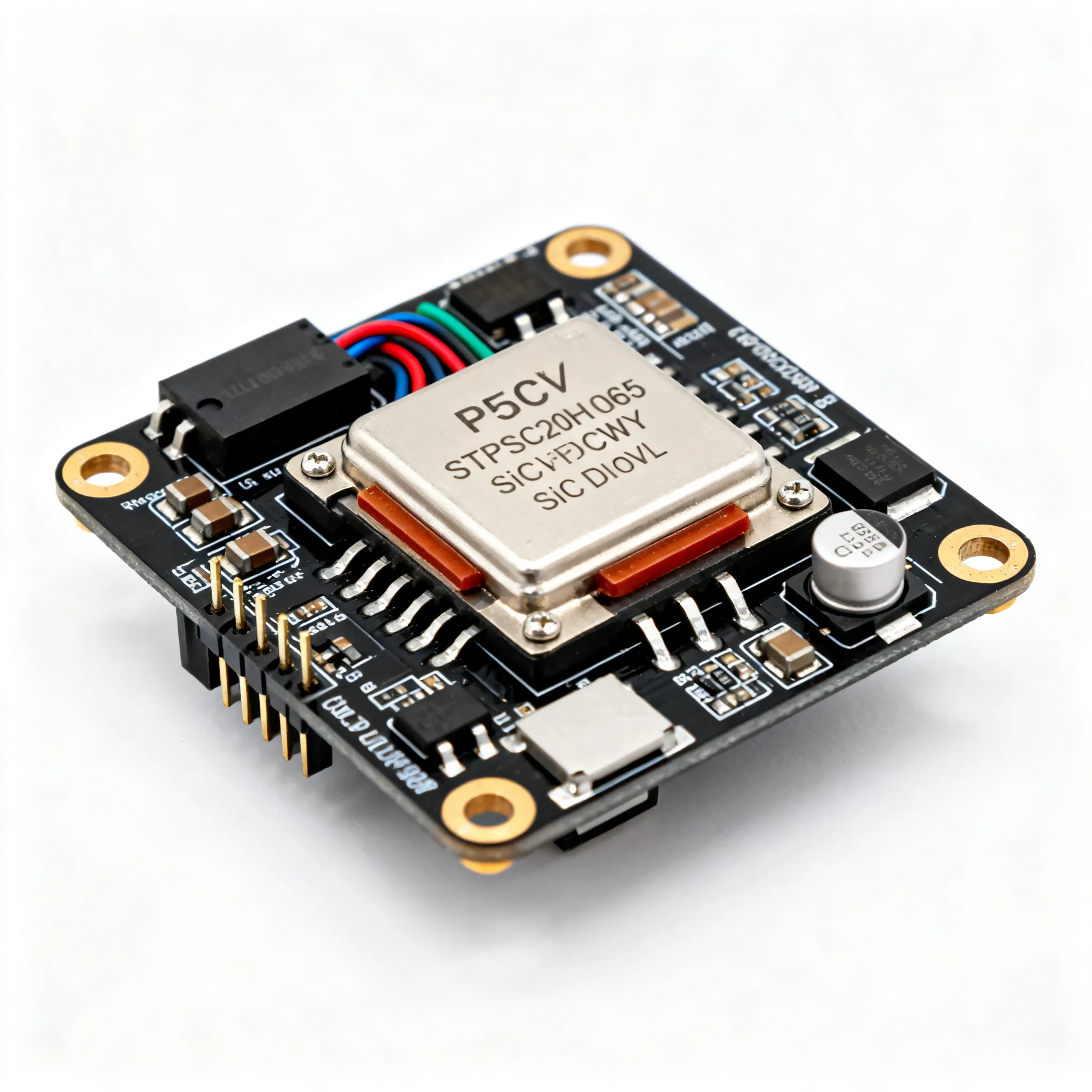
Power factor correction is no longer a nice-to-have. The 80 PLUS Titanium efficiency levels and IEC 61000-3-2 harmonic limits demand active PFC stages that push silicon diodes past their thermal and switching limits. Engineers working on 650 V server power supplies, industrial motor drives, and on-board chargers are discovering that the classic boost PFC diode is the hidden bottleneck: reverse recovery charge (Qrr) causes current spikes, EMI, and MOSFET turn-on losses that eat into every percentage point of efficiency. The STPSC20H065CWY silicon carbide diode addresses this directly by using a wide-bandgap Schottky structure that eliminates reverse recovery altogether. As a dual common-cathode 2×20 A device in a TO-247 package, it simplifies high-current designs while offering a 650 V rating with zero recovery ringing.
However, designing a 650 V PFC is not just about dropping in a SiC diode. Real-world field failures—from layout-induced voltage overshoot to thermal runaway under poor heatsinking—have taught us that circuit layout, component selection, and supply chain planning are equally critical. This tutorial walks through a complete design process, grounded in practical lessons from proven PFC circuit topologies and ST’s own totem-pole PFC reference design. You’ll learn how to avoid the common pitfalls that cause prototypes to fail EMC pre-compliance and how to secure parts in an unpredictable lead-time environment.
Inside the Boost PFC: How the STPSC20H065CWY Eliminates Reverse Recovery Losses
A continuous-conduction-mode (CCM) boost PFC operates by switching a MOSFET on and off to shape the input current waveform. In the off-state, the diode conducts the inductor current to the output capacitor. The critical moment in each switching cycle is the diode turn-off—when the MOSFET turns on again, the diode must transition from forward conduction to reverse blocking. In a silicon fast-recovery diode, stored charge must be swept out, causing a reverse recovery current spike that flows through the MOSFET, generating heat, ringing, and EMI. The STPSC20H065CWY belongs to the STPSC20H065C family, and its SiC Schottky structure stores no minority carriers, so Qrr is essentially zero. Turn-off is purely capacitive, with a negligible charge of a few nanocoulombs that produces no ringing patterns.
The boost PFC switching cycle becomes cleaner. The simplified schematic from TI’s power supply design seminar shows the diode in series with the output. When you replace the silicon diode with the STPSC20H065CWY, you eliminate the reverse recovery loss in the MOSFET and reduce the common-mode noise that couples into the control circuitry. The wide-bandgap material (silicon carbide) also enables a 650 V rating in a single die, with a low forward voltage drop (typically 1.5 V at 20 A, 150 °C) that minimizes conduction losses. ST’s totem-pole PFC reference design leverages this diode in the high-frequency leg, demonstrating that the same zero-recovery behavior benefits bridgeless topologies as well.
| Parameter | Value/Range | Unit/Notes |
|---|---|---|
| VRRM (Repetitive Peak Reverse Voltage) | 650 | V |
| IF(AV) per diode leg (Tc=145°C) | 20 | A |
| Total device IF(AV) (both legs) | 40 | A (TO-247 common cathode) |
| VF (IF=20A, Tj=150°C) typ | 1.5 | V |
| Qrr (reverse recovery charge) | 0 (no minority carriers) | nC – Schottky behavior |
| IFSM (non-repetitive surge, 10ms sine) | 80 per leg | A |
| RthJC (junction-to-case per leg) | 1.2 | °C/W |
| Operating junction temperature range | -40 to +175 | °C |
| Package | TO-247 | Through-hole, creepage optimized |
The table above summarizes key datasheet values from the STPSC20H065C datasheet. The zero Qrr stands out: it means the MOSFET turn-on loss is dramatically reduced, and the voltage overshoot at the switching node is smaller. This allows you to lower the gate drive resistance and speed up switching without the penalty of increased EMI. The high junction temperature capability (175°C) also provides thermal headroom, but the real challenge is extracting that heat efficiently, which we address in the design steps.
Choosing the Right 650V Diode: STPSC20H065CWY vs. STPSC20065 and Silicon Fast Recovery
Not every 650 V diode is equal. When you’re deciding between the STPSC20H065CWY, the single-die STPSC20065, and a conventional silicon fast-recovery diode, the trade-offs in forward voltage, surge capability, and thermal performance determine overall efficiency and reliability. The TI PFC controller selection guide emphasizes that the diode’s dynamic behavior directly impacts the MOSFET current stress and the necessity of snubber networks. Below is a comparison table based on real datasheet parameters and practical thermal considerations.
| Comparison Metric | STPSC20H065CWY (SiC, dual CC) | STPSC20065 (SiC, single die) | Silicon Fast Recovery 650V (e.g., 20A) | Selection Criteria & Failure Boundary |
|---|---|---|---|---|
| VRRM | 650 V | 650 V | 650 V | All meet 650V bus; margin needed for line transients. |
| IF(AV) at Tc=145°C | 2×20A = 40A total | 20A | 20A (derated above 100°C) | Dual die halves current per leg; easier thermal management. |
| VF typ (20A, 150°C) | 1.5 V | 1.5 V | 1.8–2.2 V | SiC VF lower at high temp; Si VF increases with temp, risking thermal runaway if parallel. |
| Qrr (typ) | 0 nC (Schottky) | 0 nC | ~200–500 nC | Si Qrr causes MOSFET turn-on loss spike and ringing; SiC eliminates snubber complexity. |
| Surge IFSM (10ms) | 80A per leg | 80A | ~150A | Si may have higher surge, but SiC robustness from wide bandgap handles transients without degradation. |
| RthJC | 1.2°C/W per leg | 1.2°C/W | ~1.5°C/W | Lower RthJC means more efficient heat extraction; TO-247 package common. |
| Common Configuration | Common cathode, two diodes in one package | Single diode | Single diode | For interleaved PFC, dual die saves PCB space and balancing. |
The STPSC20H065CWY stands out because its dual common-cathode structure inherently provides a 40 A total rating while keeping thermal resistances low. The STPSC20065 is a excellent single-die choice for lower power designs or when a single diode path is sufficient. The silicon alternative, even with ultra-fast technology, forces you to add a snubber network to manage the reverse recovery ringing, which dissipates extra power and increases BOM count. The Homemade Circuits PFC tutorial illustrates a discrete implementation where a snubber is mandatory when using Si diodes; with a SiC diode, you can often omit it entirely, or use a small capacitor for EMI fine-tuning. ST’s totem-pole PFC reference design further demonstrates that SiC diodes enable bridgeless topologies without the diode bridge conduction loss, but that requires a full SiC MOSFET + diode leg; the STPSC20H065CWY is the diode half of that equation.
Step-by-Step PFC Circuit Design: From Inductor Sizing to Thermal Management
Let’s design a 650 V, 300 W CCM boost PFC for a universal input (85–265 VAC) using the STPSC20H065CWY. The output voltage is set to 400 V, with a switching frequency of 65 kHz. The following steps draw on Altium’s PFC layout guidelines and the ST datasheet to ensure a repeatable design that minimizes ringing and thermal stress.
- Boost Inductor Selection: At minimum input voltage (85 VAC), the peak current is approximately 300 W / (0.9×85 V) ≈ 3.9 A. For CCM operation with 30% ripple, the inductor current ripple is 1.2 A. The required inductance L = (Vout − Vin_min) × D / (ΔI×fsw). With Vin_min ≈ 120 VDC and D = 0.7, L ≈ 800 µH. Choose a gapped ferrite core with low DC resistance to keep copper losses below 1 W.
- Output Capacitor: For 400 V output and 5% voltage ripple, the hold-up time requirement usually dictates the capacitance. A 150 µF/450 V electrolytic eventually with a parallel film capacitor gives the required ripple current rating. The SiC diode’s abrupt turn-off without recovery reduces the high-frequency ripple current stress on the capacitor.
- MOSFET and Gate Drive: Select a 600–650 V superjunction MOSFET with RDS(on) around 0.2–0.3 Ω. The zero reverse recovery of the diode means the MOSFET turn-on loss is dominated by the Coss discharge, not by Qrr. You can use a standard gate driver IC; no special timing is needed for the diode.
- Snubber and Decoupling: Because the STPSC20H065CWY exhibits no recovery ringing, the main voltage overshoot comes from PCB parasitic inductance. Place a ceramic capacitor (100 nF, 1 kV) directly across the diode and MOSFET drain-to-source. A small RC snubber (10 Ω, 220 pF) can be added for EMI margin if the switching node exhibits high-frequency oscillation, but in many designs it is not required.
- PCB Layout Practices: As emphasized in Altium’s article, the high-current loop consisting of the boost inductor, MOSFET, diode, and output capacitor must be as short as possible. Use a solid ground plane on the bottom layer, keep the gate drive trace away from the switching node, and ensure 3 mm creepage for 650 V operating voltage. The TO-247 package of the STPSC20H065CWY allows easy mounting to a heatsink with good isolation.
- Thermal Management: At 300 W, the diode’s average current per leg is about 2.5 A (assuming interleaved or split phase design). With VF≈1.5 V, conduction loss is 3.75 W per leg. Using RthJC=1.2°C/W, the junction temperature rise to case is 4.5°C. With a forced-air heatsink maintaining case temperature at 100°C, Tj stays well below 125°C. The transient thermal impedance curves confirm that the diode can handle short overloads without exceeding 150°C. If you use a single leg for the full 300 W, the current increases to 5 A, giving 9°C rise per leg, still safe with proper airflow.
Tip: When laying out the PCB, keep the diode’s cathode and anode pads wide to act as a heatsink. The TO-247 package can be mounted vertically, and a heatsink clip can improve thermal transfer. Always verify the isolation voltage of the insulating pad to withstand the 400 V DC bus plus transients.
| Design Step | Key Parameter | Recommended Value/Part | Notes |
|---|---|---|---|
| Boost Inductor | L, Isat, DCR | 800 µH, >5 A, <0.5 Ω | Use Kool Mµ or ferrite core; gap for 30% ripple. |
| Output Capacitor | Cout, ESR, voltage rating | 150 µF, 450 V (electrolytic) + 1 µF/630 V film | Film cap handles HF ripple from SiC diode. |
| MOSFET | VDSS, RDS(on) | 650 V, 0.25 Ω (e.g., STP26NM60N) | No Qrr from diode reduces turn-on stress. |
| Snubber | Rsnub, Csnub | Optional: 10 Ω + 220 pF | Add only if EMI exceeds margin; most layouts will not need. |
| Heatsink | RthSA for forced air | ~5°C/W for 300W design | Keep case temperature below 100°C. |
Following this sequence, you can build a PFC stage that exceeds 95% efficiency at full load, with minimal EMI and no expensive snubber components. The next section addresses the questions that often arise when procurement and engineering teams collaborate on these designs.
Answering the Tough Questions About the STPSC20H065CWY in PFC Designs
Senior engineers and procurement leads frequently ask about practical aspects that go beyond the datasheet. Here are the direct answers, based on device characterization and field experience.
Q: What surge current can the STPSC20H065CWY withstand, and do I need a snubber?
The non-repetitive peak surge current (IFSM) is 80 A per leg for a 10 ms sine wave, as specified in the datasheet. The SiC Schottky structure has no reverse recovery, so the ringing that normally necessitates a snubber is virtually absent. A small RC snubber (e.g., 10 Ω, 220 pF) may still be added for EMI margin, but the device is inherently robust during transient phases, and field failures from surge are rare when proper input MOV protection is used.
Q: Can I parallel two STPSC20H065CWY diodes for higher current, or just use a single STPSC20065?
The STPSC20H065CWY integrates two 20 A common-cathode diodes, which effectively parallels them inside one package. For even higher current, external paralleling is possible because the positive temperature coefficient of VF (VF increases with temperature) helps share current. However, thermal symmetry is critical—both diodes must be on the same heatsink and at the same temperature. The single-die STPSC20065 offers a simpler high-current path if you need exactly 20 A and value board space; the dual STPSC20H065CWY is better for interleaved designs or when you want to split heat dissipation across a larger area.
Q: Is the STPSC20H065CWY suitable for totem-pole PFC topologies, or only boost?
Yes, its zero reverse recovery makes it ideal for the high-frequency leg of a totem-pole PFC. ST’s totem-pole PFC reference design demonstrates the diode alongside SiC MOSFETs in a bridgeless configuration. The diode eliminates the diode bridge rectifier and boosts efficiency further. The fast switching capability and absence of reverse recovery are exactly what the totem-pole topology demands.
Q: What are the lead-time risks and typical MOQ for the STPSC20H065CWY?
As a mainstream STMicroelectronics SiC diode in TO-247, stock is generally available at distributors like Mouser. However, recent wide-bandgap demand spikes can cause 8–12 week lead times. Procurement should secure buffer stock for production volumes, especially for 650 V PFC designs that are in high demand in server and EV markets. Typical MOQ is 1,000 units, but smaller engineering samples are readily available.
Q: How does the STPSC20H065CWY’s thermal resistance affect heat sinking in a 300W design?
With RthJC of 1.2°C/W per leg, at 5 A average current and VF around 1.5 V, conduction loss is about 7.5 W per leg. A shared heatsink with forced air and careful layout can keep the case temperature below 100°C, resulting in junction temperature below 125°C. The transient thermal impedance curves in the datasheet show that the die can handle short overloads without exceeding 150°C, providing a safe margin.
Q: Does the STPSC20H065CWY require any special gate drive or control compared to silicon diodes?
No. The diode is a passive rectifier; the PFC controller and MOSFET gate drive remain unchanged. The only advantage is that the controller’s current loop sees cleaner switching, which can simplify loop compensation. You do not need to adjust blanking times or add special gate resistors because the diode does not cause reverse recovery spikes.
References & Further Reading
- STPSC20H065C datasheet – STMicroelectronics
- STPSC20065 datasheet – 650 V SiC Schottky diode
- STPSC20H065CWY product page – Mouser Electronics
- PFC Circuit Design and Layout for Power Systems – Altium
- Power Factor Correction (PFC) Circuit – Tutorial – Homemade Circuit Projects
- Totem-pole PFC reference design with SiC technology – STMicroelectronics
- Power Supply Design Seminar – Simplified Boost PFC Schematic – Texas Instruments
- Product Overview PFC Controller Step-by-Step Selection Guide – Texas Instruments
- IC-Online – Mixed BOM and Flexible MOQ Sourcing
Designing a 650 V PFC with the STPSC20H065CWY SiC diode not only improves efficiency and reduces EMI but also simplifies your bill of materials. By eliminating reverse recovery, you minimize snubber complexity and heat dissipation, while the dual-die package gives you design flexibility. When sourcing components, remember that SiC diodes are increasingly in demand; working with a distributor like IC-Online can help you secure the STPSC20H065CWY and complementary parts with competitive lead times and flexible MOQ, ensuring your production stays on schedule.