Your Guide to Buck-Boost Regulator Design
A buck-boost regulator is a versatile switched-mode DC-to-DC converter, merging the principles of a buck converter and a boo
A buck-boost regulator is a versatile switched-mode DC-to-DC converter, merging the principles of a buck converter and a boost converter. This unique design provides excellent voltage regulation, allowing you to produce an output that is higher, lower, or the same as the input. The buck boost regulator circuit is a superior power supply for power management challenges, especially when handling a wide input range from a source like a discharging battery. The market for this powerful converter is expanding rapidly.
💡 Market Snapshot The market for this type of DC-DC converter is projected to grow from USD 1.84 billion in 2024 to USD 5.19 billion by 2033, reflecting a strong 12.2% compound annual growth rate (CAGR).
Key Takeaways
- A buck-boost regulator makes a stable output voltage. It works even if the input voltage changes a lot.
- The duty cycle controls the output voltage. You can make the voltage higher or lower.
- Choose the right parts for your design. This includes the inductor, capacitors, and MOSFET.
- Buck-boost regulators are good for battery devices. They also work well in cars and for USB power.
THE BUCK BOOST REGULATOR CIRCUIT
To design an effective power supply, you must first understand its core structure. The buck boost regulator circuit is a powerful DC-DC converter built from a few key electronic components. Let's explore how they work together.
BASIC TOPOLOGY AND COMPONENTS
You will find four primary components in a basic buck boost regulator circuit:
- A switching MOSFET (Q1)
- An inductor (L)
- A diode (D)
- Input and output capacitors (Cin and Cout)
TWO OPERATING MODES
Your converter can operate in two main modes: Continuous Conduction Mode (CCM) and Discontinuous Conduction Mode (DCM). In CCM, the inductor current never drops to zero. In DCM, it does. DCM is common in light-load conditions.
💡 DCM Performance Note Operating in DCM affects your circuit's performance. While it can improve efficiency at very low loads, it also increases output voltage ripple. The table below shows how DCM behaves under different loads.
| Aspect | Low Power/Low Current Loads | High Power/High Current Loads |
|---|---|---|
| Efficiency | More efficient due to reduced switching losses | Less efficient due to higher peak currents |
| Output Voltage Ripple | Higher ripple voltage, creating a noisier output | Higher ripple voltage, creating a noisier output |
THE ROLE OF DUTY CYCLE
The duty cycle is the key to controlling your output voltage. It is the ratio of the MOSFET's on-time to its total switching period. You adjust the duty cycle to tell the DC-DC converter whether to buck (step-down) or boost (step-up) the input voltage. A higher duty cycle generally results in a higher output voltage.
You can calculate the required duty cycle (D) using the input voltage ($V_{in}$) and your desired output voltage ($V_{out}$). The formula is:
This equation helps you determine the precise timing needed for the buck boost regulator circuit to achieve your target output.
DESIGN CONSIDERATIONS
Making the right design choices is crucial for a successful project. You must weigh the trade-offs between different converter types and carefully select each component. This ensures your power supply is efficient, reliable, and fits your application's needs.
BUCK VS. BOOST VS. BUCK-BOOST
Your first major decision is choosing the right converter topology. While a buck-boost offers the most flexibility, it is not always the best choice. Your decision depends entirely on how your input voltage relates to your required output voltage.
- Buck Converter: Use this when your input voltage will always be higher than your output voltage. It is a step-down converter.
- Boost Converter: Choose this when your input voltage will always be lower than your output voltage. It is a step-up converter.
- Buck-Boost Converter: Select this when your input voltage can be higher than, lower than, or equal to your output voltage. This is common in battery-powered devices where the voltage drops as the battery discharges.
A buck-boost converter is more complex and physically larger than a standalone buck converter or boost converter. This increased intricacy means it often requires more components and board space. Efficiency is another key factor. When the input and output voltages are nearly identical, a standard buck-boost converter must switch rapidly between modes, leading to significant power loss.
| Converter Type | Condition ($V_{out}$ = $V_{in}$) | Ideal Efficiency | Reason |
|---|---|---|---|
| Buck Converter | MOSFET permanently on | 100% | No switching losses |
| Boost Converter | MOSFET permanently off | 100% | No switching losses |
| Buck-Boost (4-switch) | Two MOSFETs on, two off | ~100% | Minimal switching losses |
| Buck-Boost (general) | Both modes actively switching | Significantly lower | High switching losses |
SELECTING CRITICAL COMPONENTS
Once you choose a topology, you must select the right components. Your choices directly impact the performance, cost, and size of your final power supply.
Inductor (L)
The inductor stores and releases energy in every switching cycle. You calculate the required inductance based on your desired current ripple, switching frequency, and voltages. A larger inductor reduces ripple but is physically bigger and more expensive.
More importantly, you must check the inductor's saturation current (ISAT).
Your inductor must handle the peak current, not just the average. You find the peak current by adding the average DC inductor current to half of the ripple current. For designs with ferrite cores, it is wise to choose an inductor with an ISAT rating significantly higher than your calculated peak current. For example, if you calculate a peak current of 1.4 A, you might select an inductor with an ISAT of 2.3 A to ensure stable operation.
Capacitors (Cin and Cout)
The input capacitor (Cin) helps provide a steady voltage to the buck boost regulator circuit. The output capacitor (Cout) smooths the output voltage and reduces ripple, which is critical for good voltage regulation.
The most important factor for output ripple is the capacitor's Equivalent Series Resistance (ESR). A lower ESR results in lower output voltage ripple. You can estimate the ripple with a simple formula:
Output Ripple Voltage ≈ Peak-to-Peak Inductor Current × ESR
For example, a capacitor with an ESR of 0.1 Ω and a ripple current of 0.3 A will produce about 30 mV of ripple. To minimize this, you should choose capacitors with very low ESR, such as ceramic capacitors. Using a larger capacitance value also helps, but this increases cost and size.
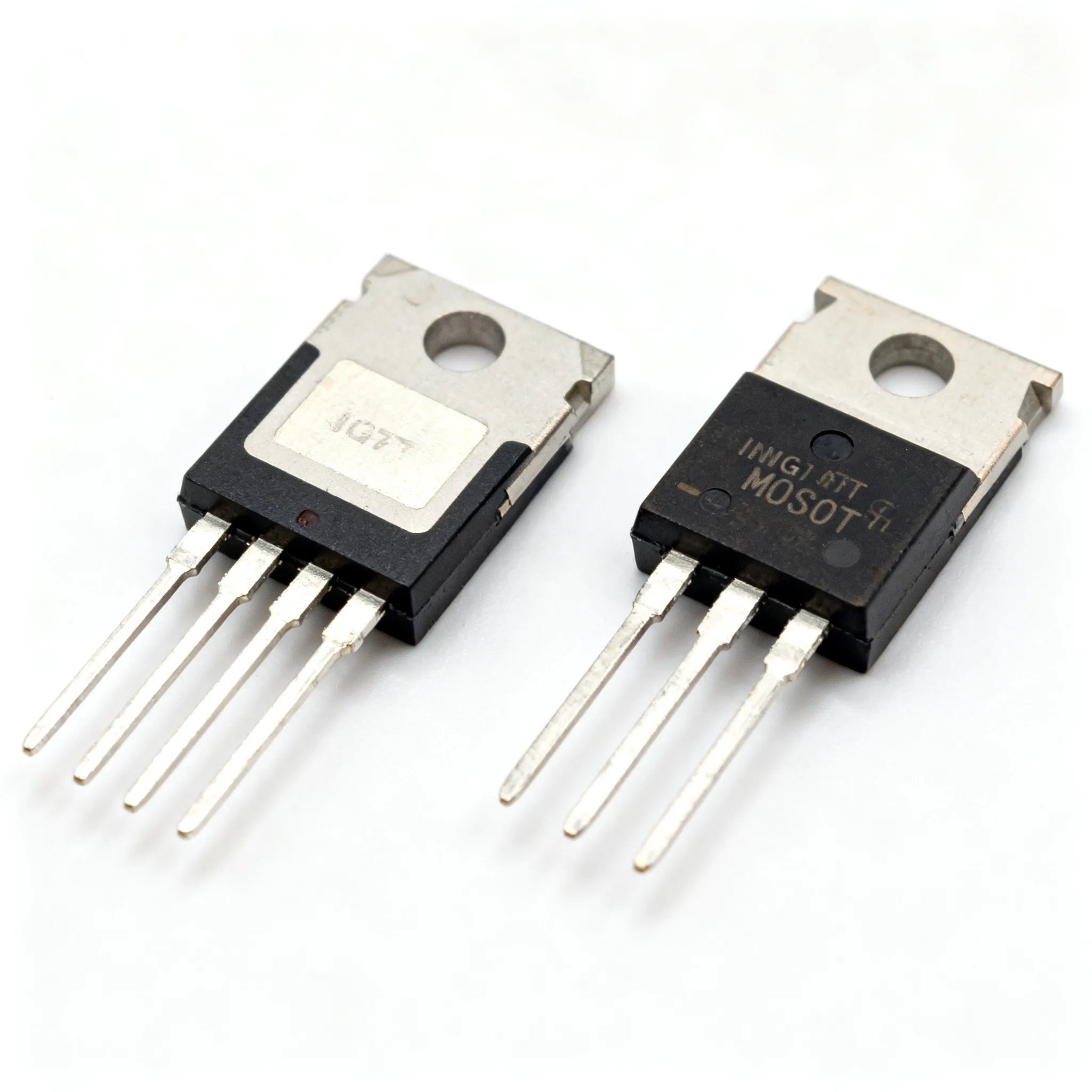
MOSFET (Q1) and Diode (D)
The MOSFET is your switch, and the diode provides a path for the inductor current when the switch is off.
- Voltage and Current Ratings: Ensure both components can handle the maximum voltage and peak currents in your circuit. The MOSFET's drain-to-source voltage rating ($V_{DS}$) must be greater than the sum of the input and output voltages.
- Switching Speed: Faster switching reduces energy loss and improves efficiency. However, very fast switching can create other noise issues.
- MOSFET On-Resistance ($R_{DS(on)}$): A lower $R_{DS(on)}$ reduces conduction losses. However, do not use it as the only selection criterion. Modern components like GaN FETs may have a higher $R_{DS(on)}$ but perform better overall due to lower switching losses. Use online loss calculation tools to compare different devices for your specific DC-DC converter.
INVERTING VS. NON-INVERTING
The basic buck-boost topology you have seen so far is an inverting converter. It takes a positive input voltage and produces a negative output voltage. This is useful for specific tasks but not for general-purpose power.
A non-inverting converter produces a positive output from a positive input. This topology is more complex, often using four MOSFETs instead of one, but it is what most people think of for a flexible power supply.
You would use an inverting buck-boost converter for a specific application that requires a negative voltage rail. Common uses include:
- Powering dual-ended sensors
- Audio amplifiers that require positive and negative supply voltages
- Creating a simple, low-cost negative voltage from a variable positive source
PRACTICAL APPLICATIONS
The buck-boost regulator's flexibility makes it perfect for many modern electronics applications. You will find these circuits in devices that need a stable output from a variable input. These applications highlight the converter's value in complex power management scenarios. Let's explore some key applications.
BATTERY-POWERED ELECTRONICS
You can see many applications for buck-boost regulators in battery-powered devices. A battery's voltage drops as it discharges. A buck-boost converter provides a constant output voltage throughout the battery's life. This makes it a reliable power supply for many applications. Common applications include:
- Smart door locks
- Connected smoke alarms
- Industrial temperature and vibration sensors
These applications demand consistent performance, which a buck-boost regulator delivers.
AUTOMOTIVE SYSTEMS
Automotive environments present tough challenges for electronics. The vehicle's voltage can drop during a "cold crank" or spike during a "load dump." A buck-boost converter handles both events seamlessly. It can step up low voltage or step down high voltage to protect sensitive systems. This makes it ideal for critical automotive applications. You will find these applications in infotainment systems and advanced LED lighting. This dc-dc converter ensures uninterrupted operation for these important applications.
💡 Did You Know? Some automotive buck-boost regulators use a special control method to reduce electronic noise. This is very important because it keeps the converter from interfering with the car's AM radio.
USB POWER DELIVERY
USB Power Delivery (USB-PD) requires a versatile power supply. The standard supports a wide output voltage range, from 5V to 20V. A simple buck or boost converter cannot handle this. You need a buck-boost converter to meet the specification. It can step the input voltage up or down to provide the correct output. This is one of the most demanding applications. The converter must also support fast role swapping, where a device switches from consuming power to providing it in microseconds. These advanced applications show the true power of buck-boost designs.
You now understand the buck-boost regulator's primary function. It delivers a stable output voltage from an input that varies above and below your target. Your design success relies on following the key steps you have learned.
Key Takeaways
- Understand the core operating principles.
- Select components based on your application's needs.
- Choose the correct topology for your circuit.
This versatile converter offers a powerful solution for solving complex power management challenges in today's electronics.
FAQ
### Why is a buck-boost less efficient than a simple buck or boost?
You see lower efficiency because a buck-boost has more components and more complex switching. These factors create higher power losses. The circuit is least efficient when your input voltage is very close to the output voltage, causing rapid switching between modes.
### How can you reduce noise and ripple in your design?
You can reduce output noise by selecting a capacitor with a very low ESR. Using a larger inductor also helps by lowering the peak-to-peak ripple current. Careful PCB layout is another key step to minimize noise in your power supply circuit.
### What is the main advantage of a 4-switch buck-boost IC?
The main advantage is its ability to produce a positive output from a positive input. This non-inverting topology is what you need for most general-purpose applications. It also offers higher efficiency when the input and output voltages are nearly equal.
### Should you use a buck-boost IC or build a discrete circuit?
For most projects, you should use an integrated circuit (IC). A buck-boost IC combines the controller, MOSFETs, and protection features into one package. This simplifies your design, saves board space, and improves reliability compared to building the circuit from discrete components.