

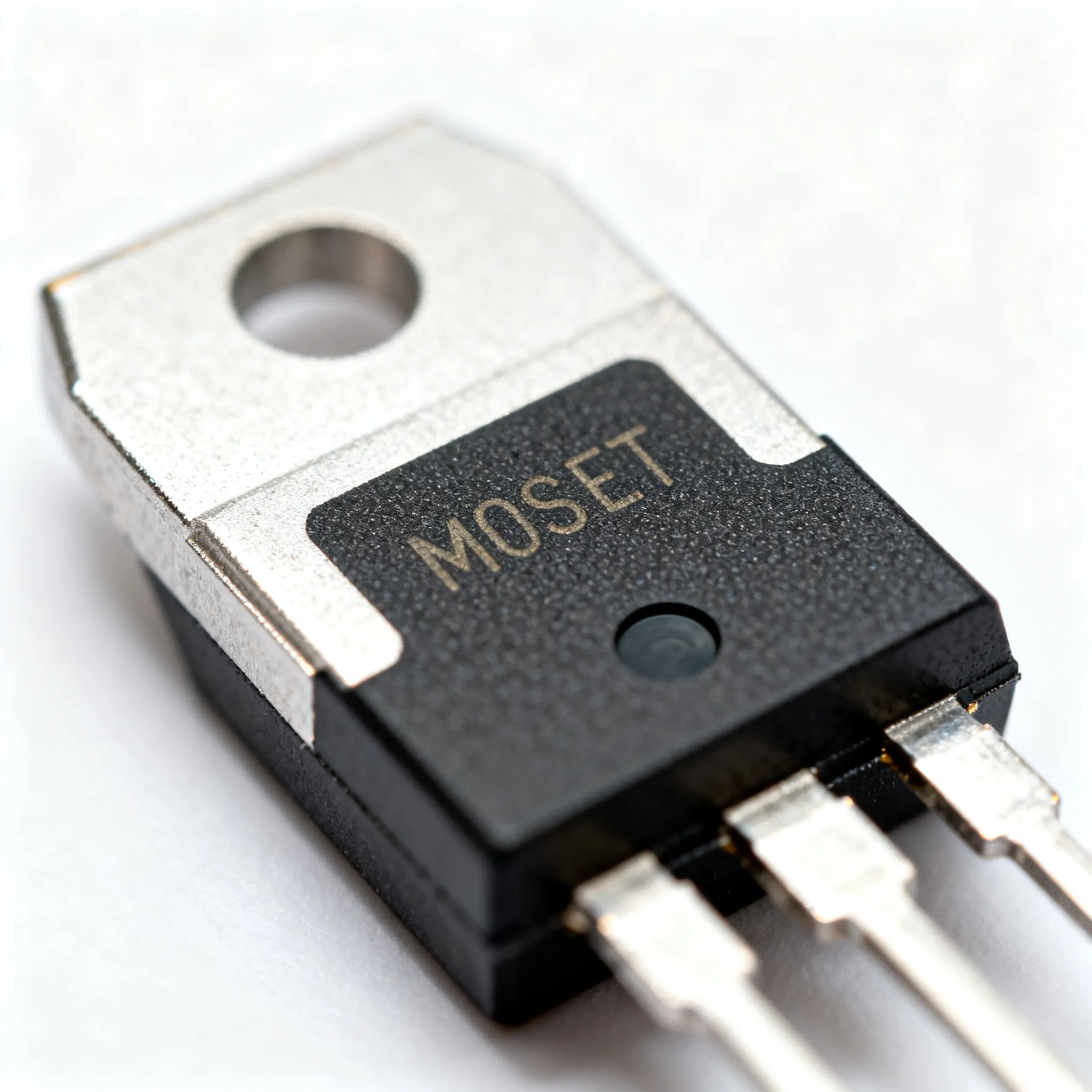
Troubleshooting the MOSFET Body Diode: Common Pitfalls and Solutions
Expert guide on Troubleshooting the MOSFET Body Diode: Common Pitfalls and Solutions. Technical specs, applications, sourcing tips for engineers and buyers.
Troubleshooting the MOSFET Body Diode: Common Pitfalls and Solutions
Every power engineer has faced the moment: a half‑bridge that worked perfectly on the bench suddenly fails in the field, leaving a shorted MOSFET and a burned gate driver. Often the root cause isn’t overvoltage or overcurrent—it’s the parasitic body diode. This intrinsic p‑n junction, formed between the drain and source of every silicon MOSFET, can turn from a harmless byproduct into a destructive element when reverse recovery, forward bias, or counterfeit parts come into play. In this article we dissect real‑world failure reports, decode the critical datasheet parameters, and compare practical mitigation strategies—from external Schottky diodes to wide‑bandgap FETs—so you can troubleshoot and prevent body diode failures before they reach your production line.
Why the Body Diode Catches Engineers Off Guard in Half-Bridge Designs
In a synchronous buck converter or an LLC resonant stage, the low‑side MOSFET’s body diode is supposed to conduct only during the dead time—a few tens of nanoseconds. But when the high‑side switch turns on, that diode must abruptly transition from forward conduction to reverse blocking. If the diode’s reverse recovery is sluggish, a massive current spike flows through both transistors, a phenomenon known as shoot‑through. The result can be an audible pop and a permanently shorted device, as reported by an engineer on the DigiKey TechForum describing a DMN67D8L‑7 failure. In that case, the MOSFET failed with a floating gate that left the transistor permanently on—a classic signature of body diode stress that propagated to the gate oxide.
Field returns often confuse body diode failures with simple drain‑source overvoltage. As noted in an analysis of six common MOSFET failure modes by Jiaensemi, distinguishing body diode breakdown from drain‑source voltage failure is difficult because the diode is a parasitic structure embedded in the same silicon. In LLC converters, the speed of the body diode directly impacts reliability: a slow diode forces hard commutation during the switching transition, leading to immediate destruction. The 4QD motor control resource lists body diode reverse recovery as one of the top ten MOSFET killers, especially in high‑frequency bridges where di/dt can exceed 1,000 A/µs.
Another subtle trap is the forward biasing of the body diode during freewheeling. In Tesla coil SSTC duty, Richie Burnett demonstrated that the body diode can be forced into conduction by resonant currents, causing excessive reverse recovery losses and eventual thermal runaway. His solution—a series Schottky diode—highlights how a seemingly benign parasitic can become the primary failure mechanism when the circuit topology works against you.
From a procurement perspective, misdiagnosed failures lead to unnecessary re‑qualification cycles, line stops, and even suspicion of counterfeit parts. When a batch of MOSFETs exhibits a 2% field return rate with shorted drain‑source, the first instinct may be to blame the silicon vendor. But without waveform analysis of the body diode’s reverse recovery, you risk replacing a good component with another that will fail in exactly the same way.
Decoding Reverse Recovery: How trr and Qrr Trigger Shoot-Through and Thermal Runaway
To troubleshoot the body diode, you must understand its reverse recovery behavior. When the diode transitions from forward conduction to reverse bias, the stored minority carriers must be swept out before the junction can block voltage. This process is characterized by three key parameters: reverse recovery time (trr), peak reverse recovery current (Irr), and reverse recovery charge (Qrr). The Infineon application note on designing with power MOSFETs explains that reverse recovery occurs whenever the diode is reverse biased while carrying a forward current, and that Qrr is the total charge that must be removed. A large Qrr translates directly into a high current spike that flows through the opposing MOSFET in a half‑bridge, effectively short‑circuiting the DC bus for the duration of trr.
The Renesas application note R07AN0007EJ0110 illustrates that during the trr period, the low‑side MOSFET is equivalently short‑circuited, resulting in a large loss. Even a “fast” body diode with trr = 100 ns can cause destructive shoot‑through if the di/dt is high enough. The peak Irr adds to the load current, and the energy dissipated in the channel of the opposing FET can exceed the single‑pulse avalanche rating. The Toshiba FAQ on body diode characteristics reminds us that Irr and trr are not constants; they depend heavily on forward current IF and the rate of current decay diF/dt. A diode that looks benign on a datasheet at 1 A/µs can become a monster at 500 A/µs.
Forward bias effects also play a role. When the body diode conducts, its forward voltage drop Vf generates heat. In circuits where the diode conducts for more than a few percent of the switching period, the resulting temperature rise can degrade trr and Qrr, creating a positive feedback loop toward thermal runaway. The SmartXProKits guide on body diode effects points out that under reverse voltage conditions, the body diode can become forward biased, causing unwanted current flow and reduced efficiency.
To put these parameters into perspective, the table below compares typical body diode characteristics for the four most common power device technologies.
| Device Technology | Typical trr (ns) | Typical Qrr (nC) | Forward Voltage Vf (V) at Rated Current | Reverse Recovery Behavior | Notes |
|---|---|---|---|---|---|
| Planar Si MOSFET (e.g., IRF540) | 200 – 500 | 1,000 – 5,000 | 1.0 – 1.5 | Slow, high Qrr; severe shoot‑through risk above 50 kHz | Legacy devices; avoid in new half‑bridge designs |
| Trench Si MOSFET (e.g., BSC009NE2LS5) | 50 – 150 | 100 – 800 | 0.7 – 1.0 | Moderate; acceptable up to 200 kHz with careful dead‑time control | Mainstream choice; check Qrr vs. temperature curves |
| SiC MOSFET (e.g., C3M0065090J) | 15 – 40 | 30 – 150 | 3.0 – 4.5 | Very fast, low Qrr; minimal shoot‑through energy | High Vf increases conduction loss if diode conducts often |
| GaN E‑HEMT (e.g., GS66508B) | 0 (no body diode) | 0 | 2.5 – 3.5 (reverse conduction via channel) | Zero reverse recovery; third‑quadrant drop is resistive + threshold | Ideal for hard‑switching half‑bridges; requires careful gate drive |
Key takeaway: If your design operates above 100 kHz and the body diode conducts during dead time, a trench MOSFET with trr under 100 ns may still be marginal. The Qrr number at your specific diF/dt and junction temperature is what matters. Always request the vendor’s characterization data at your operating conditions, not just the 25°C typical value.
Schottky Diodes, GaN, and SiC: Weighing Your Options to Tame the Body Diode
When the internal body diode becomes a liability, engineers have three practical paths: add external Schottky diodes, switch to a SiC MOSFET, or adopt a GaN FET. Each approach trades off reverse recovery, conduction loss, cost, and circuit complexity.
The classic fix, pioneered in Tesla coil inverters and documented by Richie Burnett, is to place a Schottky diode in series with the MOSFET source. This prevents the body diode from ever being forward biased because the Schottky blocks the reverse current path. A second Schottky is often added anti‑parallel to the MOSFET to provide a freewheeling path with no reverse recovery. The series Schottky approach completely eliminates Qrr from the body diode, but it adds the forward voltage drop of the Schottky (typically 0.4–0.6 V) to the conduction path, increasing losses at high current. It also requires careful layout to minimize parasitic inductance.
An alternative is to connect a Schottky diode in parallel with the MOSFET (anti‑parallel only). This reduces the current flowing through the body diode during freewheeling, thereby lowering the effective Qrr. However, the body diode still turns on momentarily, so some reverse recovery remains. This method is simpler and cheaper but only partially mitigates the problem.
Wide‑bandgap devices offer a more fundamental solution. Enhancement‑mode GaN HEMTs have no intrinsic p‑n junction between drain and source, so Qrr is truly zero. As highlighted by EEWorldOnline in their piece on body diode misconceptions, “no body diode means no QRR, making GaN suitable for half‑bridge hard switching.” This eliminates shoot‑through energy entirely. The trade‑off is a higher reverse voltage drop during third‑quadrant operation, which Power Electronic Tips explains as a resistive element plus the threshold voltage. In low‑voltage applications, this drop can be 2–3 V, leading to significant conduction loss if the device operates in reverse conduction for extended periods.
SiC MOSFETs retain a body diode, but it is a wide‑bandgap diode with extremely fast recovery (trr < 40 ns) and low Qrr. The penalty is a high forward voltage (3–4 V), which makes them less attractive for circuits where the diode conducts continuously. However, in resonant converters where the diode conducts only during dead time, SiC offers a robust, cost‑effective middle ground between silicon and GaN.
A Reddit discussion on MOSFETs without body diodes underscores the practical motivation: “Need to pass the current only one direction but a diode won’t work because of the huge forward voltage drop. MOSFET has a very low Rds…” The series Schottky approach directly addresses this by using the MOSFET’s low Rds(on) for forward conduction while blocking reverse current with the Schottky.
The table below compares these options across the metrics that matter most in a half‑bridge design.
| Approach | Reverse Recovery Charge (Qrr) | Conduction Loss Impact | Cost & Complexity | Best Use Case |
|---|---|---|---|---|
| Internal body diode only (trench Si) | Moderate (100–800 nC) | Low Vf (0.7–1.0 V) but recovery losses | Lowest cost, no extra parts | Low‑frequency (<50 kHz) or soft‑switching converters with minimal diode conduction |
| Series Schottky + anti‑parallel Schottky | Zero (body diode blocked) | Adds Schottky Vf (0.4–0.6 V) in series; freewheeling via Schottky | Moderate cost, two extra diodes, careful layout | High‑frequency hard‑switching bridges, Tesla coils, motor drives with forced freewheeling |
| Parallel Schottky only | Reduced (current sharing) | Schottky Vf in parallel reduces body diode conduction | Low added cost, one diode | Retrofitting existing designs where complete Qrr elimination isn’t required |
| SiC MOSFET | Very low (30–150 nC) | High Vf (3–4 V) but only during dead time | Higher device cost, compatible gate drive | LLC converters, high‑voltage bridges, applications needing both fast switch and fast diode |
| GaN E‑HEMT | Zero | Reverse drop 2.5–3.5 V; no diode Vf | Highest device cost, requires dedicated gate driver | MHz hard‑switching half‑bridges, compact DC‑DC converters, where zero Qrr is mandatory |
When selecting an approach, consider the duty cycle of reverse conduction. If the body diode conducts for less than 1% of the period, a SiC MOSFET’s high Vf may be acceptable. If the diode conducts continuously, a series Schottky with a low‑Vf trench MOSFET often yields the best overall efficiency. GaN is the ultimate solution for hard‑switching at hundreds of kilohertz, but the system cost and gate drive complexity must be justified.
Design and Procurement Playbook: Preventing Body Diode Failures Before They Happen
Preventing body diode failures starts at the datasheet. Jason Sachs’ guide on reading power MOSFET datasheets emphasizes the Safe Operating Area (SOA) curve and the body diode forward voltage characteristic. The SOA graph often includes a region limited by the body diode’s reverse recovery stress. If your application pushes the MOSFET into that region during switching, failure is a matter of time. Look beyond the typical Vf and trr values: request the distribution of Qrr at your specific diF/dt and junction temperature. A part with a typical trr of 80 ns might have a worst‑case of 150 ns at 125°C, which could be the difference between a reliable design and a field return epidemic.
For procurement teams, the body diode is a hidden quality indicator. Counterfeit or out‑of‑spec MOSFETs often exhibit abnormal body diode characteristics—higher Vf, larger Qrr, or inconsistent trr—because the die is a reject or a different part number. The DigiKey forum case raised the suspicion of a manufacturing defect when multiple devices failed with the same signature. While that instance may have been a genuine defect, it underscores the need to qualify every new lot. A simple curve tracer test of the body diode forward voltage and reverse recovery waveform can catch gross deviations before the parts hit the production line.
The SmartXProKits guide recommends selecting MOSFETs with a body diode designed to have a lower forward voltage drop as a first line of defense. But don’t stop there: add external clamping if the layout inductance is high. A well‑placed RCD snubber across the half‑bridge can absorb the energy that would otherwise ring through the body diode. In motor drives, a series Schottky may be mandatory if the drive’s regenerative braking forces the body diode into conduction for milliseconds at a time.
The table below maps the most common body diode pitfalls to their root causes and practical solutions.
| Pitfall | Root Cause | Symptom | Solution |
|---|---|---|---|
| Shoot‑through in half‑bridge | Slow body diode reverse recovery (high Qrr) during high‑side turn‑on | Audible pop, shorted MOSFET, burned gate resistor | Choose MOSFET with trr < 50 ns at operating diF/dt; add series Schottky; use GaN |
| Thermal runaway at high frequency | Qrr increases with temperature, causing more loss and further heating | Efficiency drops after minutes of operation; eventual short | Verify Qrr vs. temperature curve; improve cooling; reduce switching frequency or use SiC |
| Gate damage from reverse recovery current spike | High di/dt induces voltage spike on gate loop via common source inductance | Gate oxide rupture, floating gate, MOSFET stuck on | Minimize gate loop inductance; use ferrite bead on gate; add gate‑source clamp Zener |
| Counterfeit MOSFET with out‑of‑spec body diode | Unauthorized source, relabeled lower‑grade die | Random field failures, abnormal Vf or trr in sample testing | Buy only from authorized distributors; perform incoming QC with curve tracer; request batch test data |
| Misdiagnosis as overvoltage failure | Body diode reverse recovery stress looks like drain‑source overvoltage on failed device | Repeated failures after replacing MOSFET without circuit change | Capture Vds and Id waveforms during failure; look for reverse recovery current spike before voltage collapse |
Tip: When qualifying a new MOSFET supplier, ask for the body diode’s reverse recovery safe operating area (RRSOA) data. Not all manufacturers publish it, but those who do have characterized the diode’s robustness under stress. This is especially critical for LLC converters where the body diode must withstand repetitive hard commutation.
Your Toughest Body Diode Questions Answered
Q: How can I tell if a MOSFET failure is due to the body diode and not a simple overvoltage?
Look for signs of excessive reverse recovery current or thermal damage near the source bond wires. In a body diode failure, the device often exhibits a short between drain and source with a damaged gate oxide—leaving the MOSFET permanently on, as reported in the DigiKey forum case. Compare the failed waveform with the expected trr and Irr. If you see a large negative current spike just before the voltage collapses, the body diode is the prime suspect. Overvoltage failures typically show a clean avalanche breakdown without the characteristic reverse recovery signature.
Q: When should I add an external Schottky diode in series with the MOSFET source?
Use a series Schottky when the body diode would otherwise be forward‑biased during freewheeling, such as in Tesla coil SSTC duty as demonstrated by Richie Burnett, or in certain motor drives where regenerative current forces the body diode into conduction. The series Schottky blocks reverse current, preventing reverse recovery losses and shoot‑through. This is mandatory when the body diode’s Qrr would cause destructive current spikes in a hard‑switched half‑bridge.
Q: Do GaN FETs completely eliminate body diode reverse recovery problems?
Yes, enhancement‑mode GaN HEMTs have no intrinsic body diode, so Qrr is zero, making them ideal for hard‑switching half‑bridges as noted by EEWorldOnline. However, they exhibit a higher reverse voltage drop in third‑quadrant operation (typically 2.5–3.5 V) due to the channel resistance and threshold voltage. This drop must be managed thermally if the device operates in reverse conduction for a significant portion of the switching cycle.
Q: What body diode parameters are most critical for an LLC resonant converter?
Reverse recovery time (trr) and reverse recovery charge (Qrr) are paramount. In an LLC converter, the body diode conducts only during the dead time, but a slow diode can cause hard commutation and shoot‑through when the opposing switch turns on, leading to immediate failure. Look for trr below 50 ns and Qrr under 100 nC at your operating current and diF/dt. The diode’s forward voltage is less critical because conduction time is short, but its temperature dependence matters for stability.
Q: How can procurement teams ensure MOSFETs have reliable body diode performance?
Specify parts with detailed body diode characterization (trr, Qrr, Vf) from authorized distributors. Avoid unverified sources that may ship counterfeit or out‑of‑spec devices. Request batch‑level test data for critical parameters, and perform incoming inspection using a curve tracer to verify body diode forward voltage and reverse recovery waveform against the datasheet. For high‑reliability applications, work with the manufacturer to obtain reverse recovery SOA data and qualification reports that include body diode stress testing.
References & Further Reading
- Analysis of 6 Reasons for MOSFET Failure – Jiaensemi
- MOSFET Failure – Suspect Manufacturing Defect? – DigiKey TechForum
- Why Do MOSFETs Fail? – 4QD Electric Motor Control
- Why MOSFETs Fail in SSTC Duty – Richie’s Tesla Coil Web Page
- Common Misconceptions About the MOSFET Body Diode – EEWorldOnline
- Understanding MOSFET Body Diode Effects and How to Fix Them – SmartXProKits
- Common Misconceptions About the MOSFET Body Diode – Power Electronic Tips
- MOSFET Without a Body Diode – r/AskElectronics
- Application Note R07AN0007EJ0110 – Renesas (via Mouser)
- ← Previous ArticleNext Article >>
Related Articles
Choosing the Right MOSFET: A Practical Guide for Engineers in Power Applications
Expert guide on Choosing the Right MOSFET: A Practical Guide for Engineers in Power Applications. Technical specs, applications, sourcing tips for engineers and buyers.
Case Study: How Innovative Power Management ICs (PMICs) Enhance Efficiency in Consumer Electronics
Expert guide on Case Study: How Innovative Power Management ICs (PMICs) Enhance Efficiency in Consumer Electronics. Technical specs, applications, sourcing tips for engineers and buyers.
Voltage Regulator IC: Essential Buying Guide and Comparison of Leading Models for Optimal Design Choices
Expert guide on Voltage Regulator IC: Essential Buying Guide and Comparison of Leading Models for Optimal Design Choices. Technical specs, applications, sourcing tips for engineers and buyers.
 Blog
BlogOptimizing Your Bill of Materials: Cost-Effective Strategies for Sourcing Analog Devices' AD8429 Instrumentation Amplifier
Expert guide on Optimizing Your Bill of Materials: Cost-Effective Strategies for Sourcing Analog Devices' AD8429 Instrumentation Amplifier. Technical specs, applications, sourcing tips for engineers and buyers.
 Blog
BlogSelecting the Right Opto-isolator: A Guide to Choosing Between Vishay's ILQ-036 and ILQ-052 for Your Circuit Design
Expert guide on Selecting the Right Opto-isolator: A Guide to Choosing Between Vishay's ILQ-036 and ILQ-052 for Your Circuit Design. Technical specs, applications, sourcing tips for engineers and buyers.
 Blog
BlogIGBT vs MOSFET: Cost Optimization Strategies for Electronics Engineers
Expert guide on IGBT vs MOSFET: Cost Optimization Strategies for Electronics Engineers. Technical specs, applications, sourcing tips for engineers and buyers.