TSMC Unveils A14 Process Node, Targets Mass Production by 2028
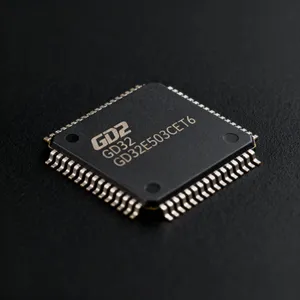
Taiwan Semiconductor Manufacturing Company (TSMC), the world’s leading contract chipmaker, has officially announced its next-generation logic process technology—A14, with mass production planned for 2028. The announcement was made at TSMC's North America Technology Symposium, where the company highlighted breakthroughs in process performance, AI enablement, and energy efficiency.
Taiwan Semiconductor Manufacturing Company (TSMC), the world’s leading contract chipmaker, has officially announced its next-generation logic process technology—A14, with mass production planned for 2028. The announcement was made at TSMC's North America Technology Symposium, where the company highlighted breakthroughs in process performance, AI enablement, and energy efficiency.
According to TSMC, the A14 node builds upon the company’s industry-leading N2 process and is designed to support the rapid transformation of artificial intelligence (AI) across devices. The technology will also enhance on-device AI capabilities, significantly improving smart functionality in future smartphones and edge computing platforms.
A14: Major Leap in Performance and Power Efficiency
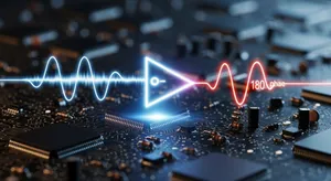
Compared to TSMC’s N2 process, which will enter mass production later in 2025, A14 is expected to deliver up to 15% faster speed at the same power, or up to 30% lower power consumption at the same speed. Additionally, logic density will improve by more than 20%, allowing designers to integrate more features into smaller chip areas.

One of the key innovations behind A14 is the enhanced NanoFlex™ Pro standard cell architecture, an evolution of TSMC’s NanoFlex™ technology used with nanosheet transistors. This upgrade allows chip designers greater flexibility and efficiency in performance tuning, energy optimization, and layout customization.
TSMC emphasized that development of A14 is progressing ahead of schedule, with early yield rates exceeding expectations—a critical benchmark that validates both the maturity of the technology and its commercial viability.
Enabling the Future of AI and Advanced Computing
The A14 node is part of TSMC’s broader roadmap to power the future of high-performance computing (HPC), AI, smartphones, automotive electronics, and Internet of Things (IoT) applications. In addition to A14, the company also revealed several updates across its specialty process technologies, advanced packaging, and 3D chip stacking platforms, all aimed at providing an integrated solution stack for customers driving the next wave of innovation.
TSMC’s Chairman and CEO, C.C. Wei, noted that TSMC's technology leadership and world-class manufacturing capabilities provide a reliable platform for customers to push the boundaries of what's possible in AI and digital transformation.