5.5V 1.5F Supercapacitor Backup Circuit Design: Step-by-Step Tutorial
Expert guide on 5.5V 1.5F Supercapacitor Backup Circuit Design: Step-by-Step Tutorial. Technical specs, applications, sourcing tips for engineers and buyers.
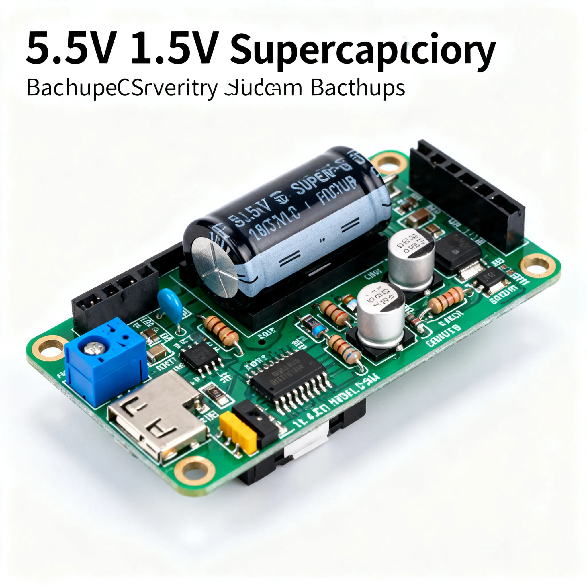
When 5V Backup Design Gets Tangled: Why a 5.5V Supercapacitor Uncomplicates Your Life
You have a 5V rail that absolutely must ride through a momentary power loss—maybe a few seconds while a supply capacitor drains, or long enough for an MCU to save critical state and shut down gracefully. The first instinct is often to stack two 2.7V supercapacitors in series. That gives you a 5.4V rating, which looks like it fits. But then comes the balancing circuit: precision resistors, an op-amp, a couple of MOSFETs, maybe a voltage supervisor, and suddenly your "simple" backup solution has a BOM count of twelve passives and three active devices. Renesas recommends 4.7kΩ balancing resistors for a 5V stack, and while passive balancing works, it burns quiescent current continuously. Active balancing is tighter but adds complexity and cost.
There is a cleaner path. On StackExchange, engineers routinely ask whether a single 5.5V-rated supercapacitor can do the job—and the answer is yes, often with fewer parts and fewer failure modes. A single 5.5V1.5F supercapacitor sits directly on the rail, charges to 5V without any balancing overhead, and delivers energy during dropout without the series-stack headaches. DigiKey's Steven Keeping has shown how a single 2.7V supercap paired with a reversible buck/boost converter can also work, but that architecture shifts complexity from balancing to converter design. The 5.5V single-cell approach eliminates both balancing and mandatory boost conversion—if your downstream load can tolerate a decaying voltage, you may need nothing more than a diode and a current-limiting resistor.
Key Takeaway: A 5.5V-rated supercapacitor like the 5.5V1.5F lets you treat backup energy storage as a single-component decision, not a subsystem design problem. This tutorial walks through the complete design flow: sizing, topology comparison, circuit implementation, and the practical questions engineers ask before committing to a prototype.
Sizing a 5.5V Supercapacitor for Your Hold-Up Time: The Energy Math That Matters
Before you pick a capacitance value, you need to characterize the load precisely. Abracon's application note on supercapacitor design emphasizes that accurate load characterization is the critical first step—everything downstream depends on it. What is the minimum operating voltage of your circuit? What current does it draw during backup? How long must it hold up?
The energy stored in a capacitor is E = ½CV², but the usable energy is only the portion between the charged voltage and the minimum operating voltage. For a 5.5V1.5F supercapacitor charged to 5V and discharged to a 2.5V cutoff, the available energy is:
Eusable = ½ × 1.5F × (5² − 2.5²) = 0.75 × (25 − 6.25) = 14.06 Joules
If your load draws 0.5A at an average of 3.75V during discharge, that's roughly 1.875W. With 14J available, you'd get about 7.5 seconds of hold-up—more than enough for a 4-second save-and-shutdown sequence. A StackExchange contributor calculated that a 5V, 0.5A, 4-second requirement needs 10J, and a 2.2F capacitor charged to 5V stores 27J. The 5.5V1.5F device at 1.5F stores about 18.75J total at 5V, comfortably above that 10J threshold.
Tip: Always add margin. Supercapacitor capacitance tolerances are typically −20%/+80% initially, and capacitance degrades over life. Apply a 30% capacitance margin and a 20% voltage derating, as discussed in the FAQ section below.
| Hold-Up Time Required (ms) | Load Current at 5V (mA) | Min. Capacitance at 5.5V Rating (F) | Suggested 5.5V1.5F Configuration | Energy Margin (%) |
|---|---|---|---|---|
| 500 | 100 | 0.10 | Single 5.5V1.5F | 1400% |
| 1000 | 250 | 0.47 | Single 5.5V1.5F | 219% |
| 2000 | 500 | 1.00 | Single 5.5V1.5F | 50% |
| 4000 | 500 | 2.20 | Two 5.5V1.5F in parallel (3.0F) | 36% |
| 5000 | 750 | 3.30 | Three 5.5V1.5F in parallel (4.5F) | 36% |
| 10000 | 500 | 5.00 | Four 5.5V1.5F in parallel (6.0F) | 20% |
The table above assumes a discharge from 5V to 2.5V with a boost converter maintaining 5V output at 85% efficiency. For applications where the load can tolerate a decaying rail voltage directly (e.g., 5V-tolerant MCUs that operate down to 3.3V), usable energy increases and the required capacitance drops. Always calculate your specific cutoff voltage before committing to a BOM.
Temperature effects matter too. DigiKey's design article notes that supercapacitor capacitance drops at low temperatures while ESR rises. If your product will cold-start at −25°C, factor in a 20–30% capacitance loss and double the ESR. These environmental deratings should be layered on top of your aging margin.
Single 5.5V Cell vs. Stacked 2.7V Cells: A Balancing Act You Can Skip
Every series-connected supercapacitor stack needs balancing. Without it, unequal leakage currents cause voltage to drift, and one cell eventually exceeds its rated voltage—shortening life or causing outright failure. The Renesas design toolkit specifies 4.7kΩ balancing resistors for a 5V system, but even that simple approach adds two resistors and a constant leakage path. Active balancing with op-amps and MOSFETs eliminates the continuous bleed current but brings its own quiescent draw, PCB area, and cost.
A single 5.5V supercapacitor like the 5.5V1.5F sidesteps the entire balancing conversation. The rated voltage (5.5V) exceeds the maximum applied voltage (5V nominal, with headroom for tolerances), so there are no series cells to drift apart. The BOM drops to one capacitor, plus optional charge-control and discharge-path components.
There is a third architecture worth comparing: the single 2.7V supercapacitor paired with a reversible buck/boost converter. DigiKey illustrates this approach, where the converter charges the cap at 2.7V and boosts it back to 5V during discharge. This recovers nearly all stored energy—a 2.7V, 5F capacitor stores 18.2J, and a boost converter can extract most of it. But the converter itself costs $1–3 in volume, occupies board space, and introduces switching noise. The table below compares the three architectures for a 5V backup application.
| Comparison Metric | Single 5.5V Supercapacitor 5.5V1.5F | Stacked 2.7V × 2 (Passive Balancing) | Single 2.7V + Reversible Buck/Boost | Selection Criteria & Failure Boundary |
|---|---|---|---|---|
| Component Count | 1 capacitor + 1 diode + 1 resistor | 2 capacitors + 2 balancing resistors + 2 zeners + 1 diode | 1 capacitor + 1 converter IC + 4–6 passives | Fewest parts = fewest failure points; 5.5V1.5F wins for simplicity |
| Balancing Required? | No (single cell) | Yes—passive or active | No (single cell) | Balancing resistors add ~10–50µA continuous drain; 5.5V cell avoids this entirely |
| Usable Energy (5V system) | 14J (5V → 2.5V, 1.5F) | ~27J (5V → 2.5V, 2×2.5F series = 1.25F effective) | ~18J (2.7V → 0.9V, 5F with boost) | 2.7V + boost extracts the most energy per farad; 5.5V cell is adequate for sub-5-second hold-ups |
| Cost (1000-up BOM) | $1.50–$3.00 | $2.50–$5.00 (caps + resistors + zeners) | $3.50–$7.00 (cap + converter + passives) | 5.5V1.5F is the lowest-cost option for moderate hold-up requirements |
| Quiescent Current | Near zero (diode leakage only) | 10–50µA through balancing resistors | 5–50µA converter shutdown current | Battery-powered designs benefit from the 5.5V cell's negligible idle drain |
| Switching Noise | None | None | Present (buck/boost switching) | Noise-sensitive analog circuits prefer the 5.5V or stacked passive approach |
| Failure Mode | Cap short or open | One cell overvoltage if balancing fails | Converter failure blocks backup | 5.5V1.5F has the simplest failure tree—single component, no active balancing |
The single 5.5V 5.5V1.5F supercapacitor is not the highest-energy solution, but it is the most direct. If your hold-up time requirement is under 5 seconds at moderate current, the simplicity advantage is compelling. For longer durations, you can parallel multiple 5.5V units—still no balancing needed—or consider the 2.7V + boost architecture if energy density is paramount.
A StackExchange discussion on supercapacitor backup circuits highlights a practical compromise: adding a 100Ω series resistor and a Schottky diode in parallel with it. The resistor limits charge current, and the diode provides a low-impedance discharge path. This simple two-component addition works elegantly with a single 5.5V cell, and we'll explore it in the next section.
Building the Circuit: Charge Control, Voltage Clamping, and Converter Selection
With the 5.5V1.5F supercapacitor selected, the circuit design breaks into three functional blocks: charging, protection, and discharge regulation. The exact implementation depends on whether your downstream load needs a regulated 5V or can tolerate a decaying rail.
Charging the Supercapacitor Without Pulling Down the Rail
A discharged 1.5F supercapacitor looks like a near-short to the 5V supply. Connecting it directly causes a massive inrush current that can sag the rail, trip overcurrent protection, or even damage the upstream regulator. The fix is a current-limiting resistor in series with the charge path. A 10Ω resistor limits peak current to 0.5A at 5V, which most 5V regulators can handle comfortably. The trade-off is charge time: with a 10Ω resistor and 1.5F capacitance, the RC time constant is 15 seconds, and the capacitor reaches 99% charge in about 75 seconds.
Engineers on StackExchange recommend placing a Schottky diode in parallel with the charge resistor—anode toward the supercapacitor, cathode toward the load. During charging, the diode is reverse-biased and the resistor limits current. During backup discharge, the diode forward-biases and provides a low-resistance path from the capacitor to the load, bypassing the resistor. A Schottky diode like the BAT54 or 1N5819 keeps the forward voltage drop to 0.3–0.4V, preserving more of the capacitor's stored voltage for the load.
Voltage Clamping: Protecting the 5.5V-Rated Capacitor
A 5V rail is rarely exactly 5.000V. With a ±5% tolerance, the rail can reach 5.25V—still safely below the 5.5V rating of the 5.5V1.5F supercapacitor. But if your supply has looser regulation or can experience transients, a clamping circuit is prudent. Industrial Monitor Direct's design guide recommends a zener diode clamp (e.g., BZX84C5V6, 5.6V) with a parallel bleed resistor of 470kΩ to 1MΩ to shunt overvoltage transients while keeping quiescent current under 10µA. For the 5.5V1.5F, a 5.3V or 5.6V zener placed across the capacitor terminals provides a hard clamp that triggers only during fault conditions.
Discharge Path: LDO vs. Boost Converter
The decision between an LDO and a boost converter hinges on the load's voltage tolerance. If your MCU or downstream circuit can operate from 3.3V to 5V, a simple LDO set to 3.3V extracts energy from the supercapacitor as it discharges from 5V down to about 3.5V (LDO dropout). This is the lowest-cost, lowest-noise solution. If the load requires a stable 5V throughout the entire backup event, a boost converter is mandatory. DigiKey's article shows a boost converter extracting energy from a supercapacitor down to 1V, recovering nearly 96% of the stored energy. Modern boost converters like the TPS61099 from TI or the MAX1724 from Analog Devices offer quiescent currents below 1µA in shutdown, making them suitable for always-connected backup circuits.
Note: If you use a boost converter, the supercapacitor's voltage drops all the way to the converter's minimum input voltage (typically 0.9–1.8V). This dramatically increases usable energy—a 5.5V1.5F discharged from 5V to 1V delivers 18.4J, versus 14J when discharged to 2.5V. The converter's efficiency (typically 80–90%) must be factored into the energy budget.
| Design Parameter | LDO-Based Discharge | Boost Converter-Based Discharge | Design Guidance |
|---|---|---|---|
| Output Voltage | 3.3V (or adjustable) | 5V (regulated) | Match to load requirements; LDO is simpler if load tolerates lower voltage |
| Usable Capacitor Voltage Range | 5V → 3.5V (LDO dropout) | 5V → 1.0V (boost min. input) | Boost extracts ~30% more energy from the same 5.5V1.5F |
| Quiescent Current | 1–5µA (typical LDO) | 0.5–5µA shutdown; 20–50µA active | LDO wins for always-on standby; boost can be enabled only during backup |
| Switching Noise | None | 10–100mV ripple at switching frequency | LDO preferred for analog sensor rails; boost acceptable for digital loads |
| Component Count | 1 LDO + 2 capacitors | 1 boost IC + inductor + 3–4 capacitors + 2 resistors | LDO: 3–4 components; boost: 7–9 components |
| Cost (1000-up) | $0.15–$0.40 | $0.80–$2.00 | LDO is cheaper; boost justifies cost when regulated 5V is mandatory |
| Recommended IC (Example) | MCP1700-3302E (Microchip) | TPS61099 (TI) or MAX1724 (ADI) | Verify dropout voltage and min. input voltage against your cap discharge range |
Complete Circuit Walkthrough
Here is a step-by-step connection sequence for a 5.5V1.5F backup circuit with an LDO output:
- Charge path: Connect a 10Ω, 0.25W resistor between the 5V rail and the positive terminal of the 5.5V1.5F supercapacitor. This limits inrush current during charging.
- Discharge bypass: Place a Schottky diode (e.g., 1N5819 or BAT54) in parallel with the 10Ω resistor—anode to the supercapacitor side, cathode to the 5V rail side. During backup, the diode conducts and bypasses the resistor.
- Reverse-polarity protection: Add a second Schottky diode between the 5V rail and the load, cathode toward the load, preventing the supercapacitor from back-feeding into the main supply when it fails.
- Voltage clamp (optional): Solder a 5.6V zener diode (e.g., BZX84C5V6) directly across the supercapacitor terminals, cathode to positive, with a 470kΩ resistor in parallel to bleed stored charge when the circuit is powered down.
- LDO connection: Connect the supercapacitor positive terminal to the input of an LDO (e.g., MCP1700-3302E). The LDO output powers the MCU or backup load. Add 1µF ceramic capacitors at LDO input and output.
- Ground: Tie all grounds—supercapacitor negative, LDO ground, load ground, and supply ground—to a single low-impedance ground plane.
- Power-good detection: Use a voltage supervisor (e.g., TPS3809 or MAX809) monitoring the 5V rail to trigger the MCU's backup routine when the main supply drops below 4.5V.
Tip: If you replace the LDO with a boost converter, move the boost converter's input to the supercapacitor side of the charge resistor and add a logic-controlled enable pin so the boost only activates when the main 5V rail is absent. This prevents the boost converter from drawing power during normal operation.
Supercapacitor Backup Circuit FAQ: Questions Engineers Ask Before Prototyping
After reviewing dozens of design forums, application notes, and field failure reports, here are the questions that come up repeatedly when engineers first work with a 5.5V1.5F backup circuit.
Q: Can I use a 5.5V supercapacitor directly without a boost converter if my downstream circuit tolerates 3.3V?
Yes, and this is one of the cleanest implementations. If your MCU or load can run down to 3.3V, you can skip the boost converter entirely. Place an LDO set to 3.3V between the 5.5V1.5F supercapacitor and the load. The capacitor voltage decays from 5V to the LDO's dropout voltage (typically 3.5V for a 3.3V LDO), at which point regulation is lost. Size the capacitor for the energy deliverable between 5V and ~3.5V. With a 1.5F capacitor, that's roughly ½ × 1.5 × (5² − 3.5²) = 9.56J. For a 100mA, 3.3V load (0.33W), that yields about 29 seconds of hold-up—plenty for most save-and-shutdown sequences.
Q: What is the minimum holding voltage for a 5V microcontroller before a clean shutdown is required?
Most 5V MCUs specify operation down to 4.5V or 4.75V, but brown-out detection (BOD) can often be configured lower. Check your specific datasheet carefully—some devices, like the ATmega328P, can operate down to 2.7V at reduced clock speeds. Industrial Monitor Direct's reference design notes that operation terminates when capacitor voltage reaches Vout + Vdropout for LDO-based solutions. If your application demands a full 5V throughout the backup period, a boost converter is non-negotiable. Configure the boost converter's enable threshold to activate when the main rail drops below 4.6V.
Q: How do I manage inrush current when charging the 1.5F supercapacitor from a 5V rail?
A series resistor is the simplest and most robust method. A 10Ω resistor limits peak inrush to 0.5A at 5V, and the power dissipated during the initial charge spike is 2.5W—but only for a fraction of a second. A 0.25W resistor handles this transient without damage. For faster charging, you can use a dedicated load switch with current limiting (e.g., TPS229xx series from TI) or a constant-current charger IC. The StackExchange community recommends placing a Schottky diode in parallel with the charge resistor to provide a low-impedance discharge path during backup. This gives you controlled charging without penalizing discharge efficiency.
Q: Does a 5.5V-rated supercapacitor need cell balancing?
No. A single cell with a rated voltage above the maximum applied voltage (5.5V > 5.25V maximum for a ±5% rail) does not require balancing. Cell balancing is exclusively needed for series-connected supercapacitors to prevent individual cell voltages from exceeding their ratings. The 5.5V1.5F is a single-cell device, so this concern is completely eliminated. Renesas' application note dedicates several pages to balancing strategies—all of which become irrelevant with a single 5.5V cell.
Q: What derating factors should I apply for temperature and aging?
Supercapacitor capacitance drops at low temperatures—typically −20% at −25°C—and ESR can double or triple. DigiKey's article emphasizes checking the datasheet for temperature effects on capacitance and resistance as one of the first design steps. For aging, derate the voltage by 20% (operate at 4.4V or below for a 5.5V-rated part) and add 30% capacitance margin to account for end-of-life degradation. If your 5.5V1.5F supercapacitor is rated for 500,000 cycles at 25°C, expect roughly half that at 65°C. Always consult the manufacturer's lifetime curves—they plot capacitance retention and ESR increase versus time at temperature and voltage.
Q: Is there a risk of overvoltage if the 5V rail is not precisely regulated?
Yes, and this is a real concern in systems with loosely regulated supplies or where hot-plug transients can occur. If the 5V supply has a tolerance of ±5%, the maximum voltage is 5.25V, which is safely within the 5.5V rating of the 5.5V1.5F. For supplies with ±10% tolerance (5.5V max), the capacitor is at its absolute limit with no margin. For higher tolerances or environments with inductive transients, add a 5.3V or 5.6V zener clamp across the capacitor terminals. A zener like the BZX84C5V6 with a 470kΩ parallel bleed resistor provides robust overvoltage protection with minimal quiescent current draw. For critical applications, consider a dedicated voltage supervisor IC that disconnects the capacitor if the rail exceeds a set threshold.
References & Further Reading
- How to Use a Single Supercapacitor as Backup Power for a 5-Volt Supply — Passive Components Blog (DigiKey article by Steven Keeping)
- How to Use a Single Supercapacitor as Backup Power for a 5-Volt Supply — DigiKey
- Supercapacitor-Based Backup Solutions: A Design Toolkit — Renesas Application Note
- 5s Backup by 1F 5.5V Super Capacitor — Electrical Engineering Stack Exchange
- Super Capacitor Backup Circuit — Electrical Engineering Stack Exchange
- Designing with Supercapacitors — Abracon Application Note (April 2024)
- Design Supercapacitor Backup Power for 5-Second MCU Hold-Up Time — Industrial Monitor Direct
- IC-Online — Mixed BOM Sourcing with Flexible MOQ for Supercapacitors and Supporting Components
Whether you are prototyping a single-unit proof-of-concept or scaling to production volumes, the 5.5V1.5F supercapacitor offers a compelling balance of simplicity, cost, and reliability. By eliminating cell balancing, minimizing component count, and providing adequate energy for most sub-5-second hold-up applications, it lets you focus engineering effort on the product—not the backup subsystem. For sourcing the 5.5V1.5F supercapacitor alongside complementary components—Schottky diodes, LDOs, boost converters, and voltage supervisors—visit IC-Online for mixed-BOM procurement with flexible minimum order quantities.