Integrated Nanoelectronic Circuits Based on Advanced Nanoscale Materials
Nanoelectronics uses advanced nanomaterials like carbon nanotubes to replace silicon, boosting processing speeds and battery life in everyday circuitry.
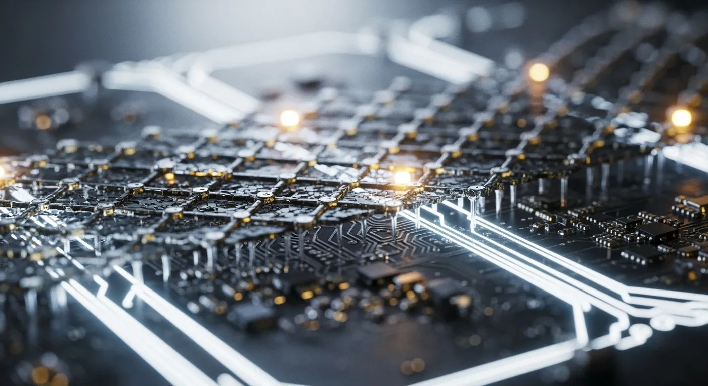
You rely on silicon-based integrated circuits daily, yet modern computer chips encounter harsh physical limits. Standard silicon transistors produce excessive heat, suffer from severe subthreshold leakage, and experience damaging short-channel effects. Advanced engineered nanomaterials supply the ideal solution to maintain continuous performance scaling. Chip designers now place one-dimensional carbon tubes and two-dimensional atomic sheets directly into hybrid circuit architectures using nanotechnology.
As an authorized HiSilicon-designated solutions partner, Nova Technology Company (HK) Limited drives integrated semiconductor innovations. Applying nanotechnology in electronics drastically lowers overall power consumption while maximizing signal efficiency. Through these advances, nanoelectronics upgrades your smart consumer devices with faster processing speeds, lower operational heat, and longer battery life.
Key Takeaways
- Advanced nanomaterials replace silicon to overcome heat and speed limits in tiny computer chips.
- Carbon nanotubes and two-dimensional crystals carry electric current much faster with far less power loss.
- Hybrid chip designs allow engineers to build smaller transistors without overheating fragile internal components.
- Everyday devices get longer battery life, cooler operating temperatures, and faster processing speeds from nanoelectronics.
Advanced Materials in Next-Generation Nanoelectronics
Carbon Nanotubes and Graphene Layers
You need superior channel materials to advance next-generation nanoelectronics beyond standard silicon limitations. Modern engineered nanomaterials offer exceptional strength and high electrical speed. Carbon nanotubes and single-layer graphene transport charge carriers without frequent collisions inside nanoscale circuits.
| Material | Carrier Mobility Range (cm²/Vs) | Comparison to Bulk Silicon |
|---|---|---|
| Graphene | 10,000 to >200,000 | More than a hundred times faster |
| Carbon Nanotubes | >100,000 | Higher than any other known semiconductor |
| Bulk Silicon | ~1,400 | Baseline |
High carrier mobility lowers total power consumption at atomic dimensions. Individual carbon nanotubes carry high electrical currents up to 10⁹ A cm⁻² with minimal internal heating. Graphene provides thermal conductivity up to 5000 W/m·K to remove heat rapidly inside compact electronics.
Two-Dimensional Atomic Crystals
Two-dimensional atomic crystals give you tight electrostatic control over ultrathin transistor channels. Atomically thin transition metal dichalcogenides solve energy leakage issues in tiny logic devices. Monolayer structures of molybdenum disulfide feature a direct energy bandgap of approximately 2.0 eV.
Engineered two-dimensional field-effect transistors achieve excellent switching characteristics:
- On/off current ratios exceed 10⁷ under standard drain voltages.
- Scaled channel lengths maintain high on/off ratios near 10⁸.
Nanotechnology helps developers build tiny logic switches with supreme energy efficiency. Nanotechnology enables ultra-low subthreshold leakage inside dense processor cores. Nanotechnology allows steady channel scaling across hybrid circuit layers. Nanotechnology transforms basic circuit designs into fast processing units. Nanotechnology integration ensures long-term functional device stability. Nanotechnology manufacturing reduces severe thermal bottlenecks. Precise nanotechnology application creates stable nanoscale conduits. Integrated nanomaterials establish high benchmarks for modern computing hardware. Layered nanomaterials optimize overall signal conduction. Functional nanomaterials protect sensitive logic gates. Functional nanomaterials replace standard bulk copper interconnects. These structured nanomaterials power modern personal electronics efficiently.
Circuit Architecture and Nanotechnology Integration
You need advanced manufacturing processes to combine new nanomaterials with existing silicon lines. As a HiSilicon-designated solutions partner, Nova Technology Company (HK) Limited advances chip-level solutions, system integration, and advanced IC architecture implementation. Modern semiconductor foundries integrate carbon channels directly above completed silicon structures using low-temperature fabrication methods. This back-end-of-line process protects underlying logic circuits from high-thermal damage. Standard manufacturing processes embed tiny channels into current silicon layouts. Specialized nanotechnology transforms basic silicon designs into high-performance hybrid systems. Modern chipmakers place dopants precisely on top of channel surfaces instead of inserting atoms internally. This surface method preserves delicate structures while enabling proper electronic functional behavior. Innovative nanotechnology provides robust physical controls during complex wafer assembly.
Hybrid CMOS and Transistor Architectures
Foundries use precise fabrication steps to build low-power channel structures over silicon wafers.
| Fabrication Technique | Key Process/Method | Purpose/Challenge Addressed |
|---|---|---|
| General BEOL Integration | Building CNT layers on top of completed silicon CMOS using low-temperature techniques | Enables integration without damaging the underlying silicon chip. |
| N-type & P-type Doping | Placing dopants precisely on top of the CNT channel rather than within it. | Achieves effective doping without disrupting the 1D CNT structure; critical for device performance. |
| Gate Dielectric Formation | Pre-treating aligned CNTs with a hafnium compound, then growing the gate dielectric directly via Atomic-Layer Deposition (ALD). | Forms a high-quality, conformal insulating layer over the nanotubes for switch operation. |
| Nanotube Array Preparation | Creating straight, parallel arrays of CNTs aligned on silicon wafers. | Provides foundational material; current challenge is achieving uniform pitch between nanotubes. |
Engineers surround ultrathin channels with gate materials to create Gate-All-Around structures. Gate-All-Around geometries give you maximum electrostatic control over thin conducting paths. A 2D field-effect transistor stops unwanted charge leakage across short channel lengths. Every nanoscale switch controls electric current flow efficiently. Applying high-k dielectrics via atomic-layer deposition creates uniform insulating walls around carbon arrays. Advanced nanotechnology improves signal switching speeds across tiny processing cores. Layered nanomaterials maintain high operational stability under tight voltage tolerances. You gain unprecedented control over tiny logical gates using structured nanomaterials. Advanced nanotechnology in electronics creates energy-efficient computing cores. Modern chip architectures rely on nanotechnology to shrink logic units without performance loss. Precise nanotechnology drives scalable circuit alignment across modern fabrication lines.
Nanoscale Interconnects and Gates
Metal contacts meet two-dimensional sheets at microscopic contact junctions. Resistance at these metal boundaries affects overall circuit performance.
| Material / Interface | Contact Resistance | Context / Condition |
|---|---|---|
| Graphene with Nickel electrodes | ~470 Ω·μm | Achieved via optimized fabrication (reordered steps, annealing) |
| Ideal Nickel electrodes on Graphene | ~30 Ω·μm | Predicted by a unified model (ab-initio simulations & measurements) |
| Epitaxial Graphene on SiC (edge contact) | ~67 Ω·μm | Using a scalable tri-layer resist fabrication method |
| Epitaxial Graphene on SiC (edge contact) | < 50 Ω·μm | At high carrier densities, using the same scalable method |
| MoS₂ FETs | Not quantified as Ω·μm | Method demonstrated versatility, achieving high ON/OFF ratios (> 10⁶) |
Optimized fabrication techniques lower interface resistance in next-generation nanoelectronics. Engineers use edge contacts to lower current barriers along microscopic signal paths. Scalable tri-layer resist methods yield contact resistance below 50 Ω·μm at high carrier densities. Lower contact resistance reduces power loss across atomic channels. Every ultra-small component operates with minimal signal delay. Advanced nanomaterials replace traditional copper wires inside sub-nanometer interconnect networks. Modern nanotechnology enables faster signal propagation between dense logic units. Sophisticated nanotechnology allows clean integration across complex hybrid chip architectures. These structural breakthroughs advance high-speed processing for commercial electronics.
Everyday Circuit Applications of Nanoelectronics
Advanced circuit designs change how you use personal hardware every single day. Modern nanoelectronics bridges the gap between atomic laboratory research and real commercial products.
Wearables and Low-Power Mobile Circuits
You interact with small smart sensors continuously throughout your daily routines. Compact hardware like smartwatches and personal health trackers demands efficient signal processors. Advanced nanotechnology allows semiconductor engineers to shrink individual logic gates down to sub-nanometer scales. Smaller logic channels reduce overall power consumption while maintaining rapid signal processing speeds.
Connected iot networks rely heavily on these tiny integrated systems. Smart mobile devices run complex health monitoring algorithms directly on chip without exhausting internal battery reserves. Integrating engineered two-dimensional channel layers grants ultra-low power consumption for continuous biometric tracking. You wear lighter smartwatches because smaller batteries easily sustain multi-day operations without requiring frequent recharging.
Smartphones benefit immensely from advanced channel geometries and low-leakage logic gates.
- Smart sensors gather vital body metrics continuously.
- Edge iot nodes process local data instantly.
- Portable iot modules transmit continuous wireless telemetry.
These integrated circuits lower internal heat generation across dense mobile packages. Lower thermal dissipation keeps your handheld hardware cool during intensive wireless data transfers. Modern consumer electronics perform complex computational tasks smoothly without unexpected battery drains. Lightweight mobile devices deliver continuous background processing while preserving physical comfort during extended daily usage.
Battery life remains important when you operate personal tracking devices. Microscopic energy-harvesting circuits convert kinetic motion and temperature differences into electricity on device. Power management units distribute harvested energy efficiently to onboard sensor arrays. You receive uninterrupted real-time health data during fitness activities. These system optimizations extend hardware longevity while maintaining tiny physical dimensions.
High-Performance Computing and Displays
You demand faster speeds and crisp visual displays from personal computers. Next-generation gaming hardware and high-performance electronics require high current throughput across ultra-dense microprocessors. Precision nanotechnology provides the foundational structural base for high-density computer processors. Carbon-based transistors conduct electric charges rapidly with minimal internal resistance across dense circuit blocks. Higher carrier mobility elevates overall processing speed across modern multi-core computing chips.
Advanced displays use tiny material structures to produce vivid visuals on flexible, lightweight surfaces.
| Display Component | Nanotechnology Implementation | Functional Advantage for End-Users |
|---|---|---|
| Quantum Dot Layer | Atomically precise semiconductor nanocrystals | Delivers bright, highly accurate color emission |
| Flexible Matrix | Ultrathin two-dimensional transistor arrays | Enables foldable screens with high mechanical endurance |
Foldable smartphones use these flexible quantum dot displays alongside ultrathin thin-film transistors. Incorporating structured nanotechnology into display backplanes prevents performance degradation over thousands of folding cycles. Modern displays dissipate minimal thermal energy, so your screens remain comfortable to hold during long viewing sessions.
High-speed workstations demand continuous computational efficiency. Advanced nanotechnology allows semiconductor foundries to build compact interconnect channels. These tiny conduits prevent signal degradation when processor cores transfer massive files. Lower electrical resistance prevents thermal spikes during prolonged computing workloads. You experience seamless multitasking performance when running demanding applications.
Engineers replace bulky copper wires with atomic layers to optimize data paths. Applied nanotechnology eliminates signal bottlenecks inside graphics engines and artificial intelligence accelerators. Consequently, your desktop processors deliver maximum computing throughput without requiring massive cooling equipment. You enjoy lighter mobile devices, faster application launches, lower operational heat, and extended battery runtimes.
You now witness the semiconductor industry shift from geometric silicon scaling to material-centric chip design. Advanced nanomaterials solve core thermal bottlenecks by reducing operational heat generation across dense logic arrays. Atomically thin channels deliver superior subthreshold performance while driving extreme footprint reduction inside microscopic computer chips. Advanced nanotechnology enables these vital breakthroughs, creating energy-efficient nanoelectronics for future hardware applications.
| Source Category | Commercialization Timeline |
|---|---|
| Optimistic Startups | Around 2030 |
| General Industry Consensus | Latter half of the 2030s |
| Broader Industry Roadmap | Beyond 2038 |
Foundries will gradually integrate these structured nanomaterials into commercial fabrication lines. Applied nanotechnology will soon transform your everyday personal electronics completely.
FAQ
What physical limits affect standard silicon integrated circuits?
Standard silicon transistors produce excessive heat during operation. They suffer from severe subthreshold leakage and short-channel effects. These physical limitations stop engineers from scaling traditional computer processors down to smaller dimensions without sacrificing overall energy efficiency.
How do carbon nanotubes improve transistor channels?
Carbon nanotubes transport charge carriers without frequent internal collisions. Their high carrier mobility drastically lowers operating power and parasitic capacitance. Transistors using carbon nanotube channels conduct electric currents efficiently while generating minimal heat across dense logic arrays.
Why do chip designers use two-dimensional atomic crystals?
Atomically thin crystals offer precise electrostatic control over ultrathin transistor channels. Materials like molybdenum disulfide feature a direct bandgap that stops unwanted energy leakage. You get highly efficient logic switches that maintain high signal ratios inside microscopic computer chips.
What advantage does a nem device provide in low-power circuits?
A nem mechanical structure provides abrupt physical switching with zero off-state current leakage. Combining a nem component with advanced two-dimensional materials increases overall circuit efficiency. You achieve reliable signal control across ultrathin hybrid processing cores.