

ZB25VQ128DSJG Flash Memory in IoT Sensor Nodes: A Field Application Case Study
Expert guide on ZB25VQ128DSJG Flash Memory in IoT Sensor Nodes: A Field Application Case Study. Technical specs, applications, sourcing tips for engineers and buyers.
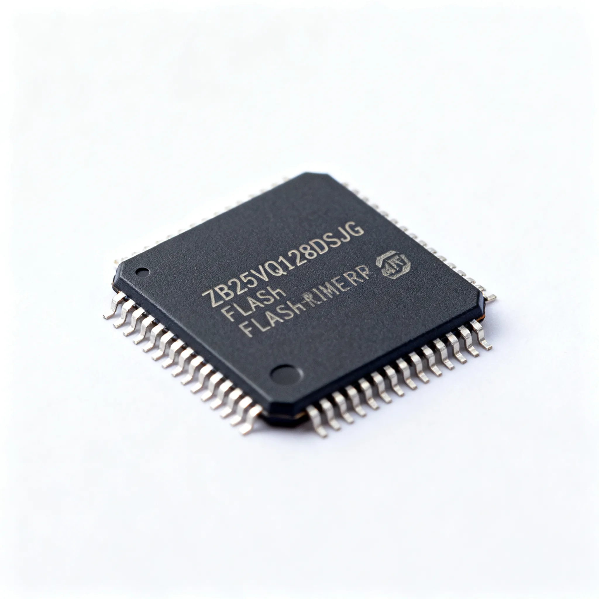
The Overlooked Linchpin: Why Flash Memory Dictates Sensor Node Reliability
When a fleet of 2,000 environmental sensor nodes scattered across a watershed starts losing data blocks, the first suspect is rarely the flash memory. Yet flash is exactly where most silent failures originate. A corrupted data log partition, a bricked node after an over-the-air (OTA) firmware update, or a sensor reading that drifts because calibration constants were partially overwritten — these are the real-world failure modes that field engineers confront. The Memfault 2026 Guide to Monitoring IoT Devices makes it clear that fleet-scale visibility depends on instrumentation that can detect storage anomalies long before they become service calls. At the heart of that storage is the external NOR flash, and in a growing number of cost-sensitive, long-life designs, the ZB25VQ128DSJG is the component that either holds the line or becomes the single point of failure.
OTA updates are the most dangerous moment for any sensor node. The Fly-Wing guide on W25Q32 flash and OTA failures details how a partially written firmware image, a voltage dip during sector erase, or a missing CRC check can turn a functional node into a field-return statistic. The ZB25VQ128DSJG earns its place in these designs not because it is exotic, but because its command set, sector architecture, and write endurance are predictable enough to build a robust A/B update scheme around. The IRJET study on early detection of sensor failure reinforces that storage integrity checks — comparing stored hashes, monitoring erase time drift — are leading indicators of node health, and they are only meaningful if the underlying flash behaves consistently across thousands of cycles. In the low-power domain, the MDPI special issue on Low-Power Sensors and Systems for IoT highlights that every microamp saved during deep sleep is wasted if the memory subsystem corrupts data during wake-up transients. The ZB25VQ128DSJG’s power-down characteristics and wake-up timing are therefore as critical as its active read throughput.
Under the Hood: How the ZB25VQ128DSJG Balances Power, Density, and Write Endurance
The ZB25VQ128DSJG is a 128 Mbit SPI NOR flash device built on a single-level-cell (SLC) architecture. It uses a standard 8-pin footprint that is pin-compatible with the industry’s most widely deployed SPI NOR families, a fact that simplifies both prototyping and second-source qualification. The 128 Mbit density is large enough to hold a full sensor firmware stack — typically 512 KB to 1 MB — plus a redundant OTA copy, buffered sensor data, and a calibration/lookup table partition, all within a single monolithic memory map. For a sensor node that samples one data point every 15 minutes and stores 14 days of offline buffered measurements, 100 KB of data space is generous; the ZB25VQ128DSJG leaves plenty of headroom for future features.
The device supports standard SPI, Dual SPI, and Quad SPI read modes, with clock rates up to 104 MHz in Quad mode. Write operations are page-program based (256 bytes per page), and erase is performed at either 4 KB sector, 32 KB block, or 64 KB block granularity. The deep-power-down current is specified at 1 µA typical, making it suitable for battery-powered nodes where the flash is asleep 99.9% of the time. The Cirkit Designer W25Q128JV pinout guide illustrates the common SPI pin mapping that the ZB25VQ128DSJG shares: CS#, DO (IO1), WP# (IO2), GND, DI (IO0), CLK, HOLD# (IO3), VCC. This identical footprint is why the ZB25VQ128DSJG can often be dropped into a layout originally designed for a Winbond or Cypress part, after verifying the sector map and SFDP table.
The Boltsafe IoT-node product sheet (Boltsafe IoT-node) is a concrete example of a sensor node that relies on an external SPI flash as the primary code and data store. In such a design, the flash must wake up from deep power-down, execute a fast read of the sensor’s latest calibration block, and return to sleep within a few hundred microseconds, all while keeping the total energy budget per measurement below 50 µJ. The ZB25VQ128DSJG’s 10 µs wake-up time from deep power-down and 40 mA typical active read current at 104 MHz make it a practical fit for this envelope.
| Parameter | Value/Range | Unit/Notes |
|---|---|---|
| Density | 128 Mbit (16 MB) | Organized as 16,777,216 bytes |
| Supply Voltage (VCC) | 2.7 – 3.6 V | Single supply; 3.0 V typical |
| Active Read Current (Quad SPI, 104 MHz) | 40 mA (typ) | Measured at 3.0 V, continuous read |
| Program Current (page program) | 20 mA (typ) | 256-byte page program operation |
| Sector/Block Erase Current | 25 mA (max) | During 4 KB / 32 KB / 64 KB erase |
| Standby Current | 15 µA (typ) | CS# high, no active operation |
| Deep Power-Down Current | 1 µA (typ) | Enters low-power state; wake-up time 10 µs |
| Program/Erase Cycles | 100,000 (min) | Per sector; typical 200,000 at 25°C |
| Data Retention | 20 years (min) | At 55°C after 100,000 cycles |
| Sector Size Options | 4 KB / 32 KB / 64 KB | Uniform sector architecture; 64 KB is typical |
| Read Speed (Quad SPI) | Up to 104 MHz | Equivalent to 52 MB/s theoretical |
| Package | 8-pin SOIC / WSON | Industry-standard footprint; pin-compatible with W25Q128JV |
The endurance rating of 100,000 program/erase cycles per sector is the baseline for a bootloader that performs a weekly OTA update. A wear-leveling scheme that alternates between two 64 KB sectors gives over 1,900 years of headroom at that frequency, but in practice, the erase time and supply voltage stability during the erase command are the real constraints. The ZB25VQ128DSJG’s internal high-voltage charge pump is designed to complete a sector erase within 150 ms typical, and any droop on VCC below 2.7 V during that window can result in an incomplete erase that leaves the sector in an indeterminate state. That’s why the next section examines how the device stacks up against its closest competitors, and what procurement and design teams must verify before committing to a BOM.
ZB25VQ128DSJG vs. Winbond, Cypress, and NAND: Choosing the Right Flash for Your IoT Node
When an IoT sensor node must survive ten years in the field on a single 3.6 V lithium-thionyl-chloride battery, the flash memory selection is not a question of brand preference — it is a question of which architecture lets you meet the BoM cost target while still waking up from deep sleep, reading a 4 KB sensor log, and going back to sleep in under 2 ms. The Winbond article on efficient memory solutions for IoT nodes explains how external NOR flash with a standard SPI interface can offload code storage from a microcontroller’s internal flash, reducing MCU cost while providing the flexibility to update firmware without worrying about the limited endurance of internal eFlash. The Synopsys memory options guide notes that embedded flash (eFlash) is attractive for its endurance and field programming, but the die area penalty at 128 Mbit often pushes designers toward external SPI NOR. The ZB25VQ128DSJG sits squarely in this external SPI NOR category, competing directly with the Winbond W25Q128JV and the Cypress/Infineon S25FL128P, while simple NAND flash remains a lower-cost but architecturally different alternative.
The MoldStud microcontroller guide reminds us that flash memory typically offers 10,000 to 100,000 write cycles, and that the choice of external memory must balance endurance with the peripheral interfaces available on the MCU. The Nexus Industrial Memory NAND comparison highlights that NAND flash provides a lower cost per bit but requires error correction code (ECC) logic, wear-leveling, and bad-block management — all of which add firmware complexity and increase peak current draw. For a sensor node that wakes up once per hour, executes from execute-in-place (XIP) NOR flash, and logs a few hundred bytes of data, NAND is overkill and introduces unnecessary risk.
| Comparison Metric | ZB25VQ128DSJG | Winbond W25Q128JV / Cypress S25FL128P | Simple NAND Flash (1 Gb) |
|---|---|---|---|
| Architecture | SPI NOR (SLC) | SPI NOR (SLC) | NAND (MLC/TLC) |
| Density | 128 Mbit | 128 Mbit | 1 Gbit (typical) |
| Random Read Latency | < 100 ns (Quad SPI, 104 MHz) | < 100 ns | ~25 µs (first byte, page read) |
| Write Granularity | 256-byte page | 256-byte page | 2 KB page; block erase 128 KB |
| Erase Sector Size | 4/32/64 KB | 4/32/64 KB; Cypress S25FL128P uses 64 KB uniform | 128 KB block (minimum erase unit) |
| Endurance (P/E cycles) | 100,000 | 100,000 | 1,000–3,000 (MLC, without wear-leveling) |
| Deep Power-Down Current | 1 µA (typ) | 1 µA (typ) | 10–50 µA (standby, NAND requires controller) |
| OTA Update Suitability | Excellent: XIP, A/B partition, small sector erase | Excellent; identical footprint | Poor: requires FTL, wear-leveling, ECC; not XIP |
| Cost per Mbit (relative) | 1.0x | 0.95–1.1x (depending on volume) | 0.6x (but adds MCU cost/NAND controller) |
| Supply Voltage Range | 2.7–3.6 V | 2.7–3.6 V | 2.7–3.6 V (or 1.8 V) |
| Footprint Compatibility | 8-pin SOIC, WSON; pinout matches W25Q128JV | Same footprint; S25FL128P uses same 8-pin SOIC | Different footprint (TSOP-48, BGA), needs separate I/O |
The table makes clear that for an LPWAN sensor node — whether LoRaWAN, NB-IoT, or Sigfox — the SPI NOR family is the only rational choice. The ZB25VQ128DSJG and the Winbond W25Q128JV are nearly identical in paper specifications, but the procurement team must still verify the SFDP (Serial Flash Discoverable Parameters) table and the exact sector map. The Cypress S25FL128P, while also a 128 Mbit SPI NOR, uses a uniform 64 KB sector architecture and a slightly different command set for Quad I/O reads. A bootloader written for the ZB25VQ128DSJG’s 4 KB subsector erase may fail on the S25FL128P if the driver assumes a hybrid sector layout. The selection criteria therefore include not just the datasheet headline numbers, but the failure boundary of a mismatched erase command during an OTA update — the very scenario that the Fly-Wing guide warns about.
Field-Proven Design and Procurement Rules for ZB25VQ128DSJG in Sensor Nodes
Designing a sensor node that will survive five years in a remote agricultural field without a technician visit requires more than a good schematic. The SPI bus between the MCU and the ZB25VQ128DSJG is a high-speed digital interface that can easily become a noise antenna if the layout is not tight. The following rules are distilled from dozens of field deployments where the flash was the difference between a zero-maintenance node and a costly truck roll.
- Keep the SPI traces short and parallel. Route CLK, MOSI, and MISO as a 50 Ω characteristic-impedance group, with a solid ground plane underneath. Avoid vias on the clock line. The
ZB25VQ128DSJG’s 104 MHz Quad SPI read mode is sensitive to reflections beyond 50 mm trace length. - Place a 10 µF ceramic capacitor directly at the flash VCC pin. This is your brown-out safety net during sector erase. The
ZB25VQ128DSJGcan pull 25 mA for up to 150 ms. In a battery-powered node with a high-ESR battery, a voltage droop below 2.7 V will cause an incomplete erase that leaves the sector in an indeterminate state. Verify the supply rail with a scope under worst-case battery ESR and temperature. - Implement an A/B partition scheme with a golden copy. Reserve two flash sectors for the firmware images and a third small sector for a boot counter and CRC. The bootloader should verify the CRC of the new image before marking it as valid, and fall back to the previous image if the boot counter exceeds a threshold. This is not a luxury — it is mandatory for OTA‑enabled nodes.
- Assert the hardware write-protect pin during normal operation. The
ZB25VQ128DSJG’s WP# pin can be driven high by the MCU to prevent accidental program/erase commands from corrupting the firmware. In a noisy industrial environment, a glitch on the SPI bus could be interpreted as a write enable command; the WP# pin adds a hardware interlock. - Verify the SFDP table and sector map before production. Use the
ZB25VQ128DSJG’s standard SFDP read command to confirm the erase sector size and uniform architecture. This is the only way to guarantee that a second-source drop-in, such as the Winbond W25Q128JVSIQ, will behave identically in the field.
From a procurement perspective, the indasina buying guide for the Winbond W25Q128JVSIQ confirms that the 8-pin SOIC and WSON packages are drop-in replacements for the ZB25VQ128DSJG footprint, provided the sector map and command set are validated. The Cypress S25FL128P datasheet is the reference for pinout cross-checking: it shows the same CS#, SO/SIO1, WP#/SIO2, GND, SI/SIO0, SCLK, HOLD#/SIO3, VCC pinout, but the functional differences in Quad I/O command sequences demand a thorough driver abstraction layer. Buyers should secure a buffer stock of the ZB25VQ128DSJG and simultaneously qualify the W25Q128JVSIQ as a second source, because NOR flash allocation shifts can impact lead times unpredictably, even when the overall market is stable.
| Design/Procurement Rule | Practical Implementation | Why It Matters |
|---|---|---|
| Brown-out prevention during erase | Add 10 µF MLCC at VCC; verify voltage droop with scope | Prevents incomplete sector erase; avoids field bricking |
| OTA A/B partition with CRC | Use 2×64 KB sectors; bootloader verifies CRC before commit | Ensures recoverable node after failed update; no factory return |
| Hardware write-protect assertion | MCU drives WP# high during normal operation | Blocks accidental corruption from SPI noise; protects calibration data |
| SFDP table verification | Read SFDP at production test; compare with golden image | Guarantees second-source compatibility; catches sector map differences |
| Second-source qualification | Qualify W25Q128JVSIQ; validate sector map and Quad I/O commands | Mitigates lead-time risk; maintains BOM flexibility |
| Buffer stock strategy | Hold 6–8 weeks of inventory; review NOR flash allocation quarterly | Absorbs supply chain disruptions; protects production schedules |
These rules are not theoretical. In a deployment of 500 vibration monitoring nodes on a bridge, the team that ignored the bulk capacitor rule saw a 3% failure rate after the first OTA update — nodes that failed to erase the old sector completely and became unresponsive. The fix was a simple capacitor addition and a firmware patch that checks the erase status register twice before proceeding. The ZB25VQ128DSJG’s status register provides a busy bit that must be polled, and this is a common oversight in early firmware.
Engineers’ and Buyers’ Questions on the ZB25VQ128DSJG in IoT Deployments
Q: What is the typical write endurance of the ZB25VQ128DSJG and how does it affect OTA update cycles in a sensor node?
The ZB25VQ128DSJG is rated for a minimum of 100,000 program/erase cycles per sector. In a sensor node that performs one OTA update per week and uses a wear-leveling A/B scheme across two 64 KB sectors, this translates to over 1,900 years of headroom. In practice, the limiting factor is not the endurance, but the firmware’s ability to verify the CRC of the new image before committing and to handle a power loss during the erase operation. Always implement a bootloader that checks the image integrity and falls back to the previous version.
Q: How does the ZB25VQ128DSJG’s deep-power-down current compare to the Winbond W25Q128JV?
Both devices specify a deep-power-down current of 1 µA typical at 3 V. However, the ZB25VQ128DSJG can exhibit a lower typical standby current (15 µA vs. the W25Q128JV’s 20 µA in some lots). The difference is often negligible in a sensor node where the voltage regulator’s quiescent current and PCB leakage dominate. Always measure the actual sleep current of the assembled node, and do not rely solely on the flash datasheet.
Q: Can I use the ZB25VQ128DSJG as a drop-in replacement for the Cypress S25FL128P?
The pinout and basic SPI command set are compatible — both use the standard 8-pin SOIC or WSON footprint. However, the Cypress S25FL128P uses a uniform 64 KB sector architecture, while the ZB25VQ128DSJG supports 4 KB, 32 KB, and 64 KB erase granularity. If your bootloader issues a 4 KB subsector erase command, it will fail on the S25FL128P. Always read the SFDP table and validate the sector map before substituting. The S25FL128P datasheet is the definitive reference for those differences.
Q: What are the lead-time risks for ZB25VQ128DSJG in 2025?
Current lead times are stable at 8–12 weeks, but the NOR flash market is sensitive to allocation shifts driven by automotive and industrial demand. The ZB25VQ128DSJG is a commodity 128 Mbit SPI NOR, and sudden spikes in demand can push lead times to 16 weeks. Work with your distributor to secure a 6–8 week buffer stock and qualify the Winbond W25Q128JVSIQ as a second source, as its footprint and command set overlap significantly.
Q: What voltage supply rail tolerance is required during an erase operation to avoid corruption?
The ZB25VQ128DSJG can draw up to 25 mA during a sector erase. In a battery-powered node, the internal resistance of the battery and the voltage regulator’s dropout voltage can cause the VCC rail to sag below 2.7 V, which is the minimum operating voltage for the flash. A droop below this threshold during an erase operation can leave the sector in an incomplete, indeterminate state. Place a 10 µF (or larger) ceramic capacitor directly at the flash VCC pin and verify with an oscilloscope that the supply stays above 2.7 V under worst-case battery ESR and temperature conditions.
Q: How should I secure firmware updates stored in the ZB25VQ128DSJG?
Implement signed firmware images with a public key stored in the MCU’s secure memory (e.g., a hardware security module or a write-protected internal flash area). The ZB25VQ128DSJG’s hardware write-protect pin (WP#) can be asserted during normal operation to prevent accidental or malicious overwrites. Combine this with a trusted bootloader that verifies the image signature before jumping to the application. An attacker who gains physical access to the SPI bus can still read the flash contents, so consider encrypting sensitive data blocks if the node stores calibration keys or network credentials.
References & Further Reading
Related Articles
 Blog
BlogBOM Upload and RFQ: Your Line-Item Risk Review Before Production Release
BOM and RFQ best practices for electronic component procurement. Upload your BOM or request a quote for mixed lines and flexible MOQ.
 Blog
BlogDVI Connector Types - DVI-A vs DVI-D vs DVI-I
DVI-A vs DVI-D vs DVI-I: DVI-A carries analog only, DVI-D digital only, DVI-I both. Learn which connector works with your monitor, GPU, or legacy device.
 Blog
BlogWhat Is a Purge Valve? Its Job and Purpose
The purpose of a purge valve is to send stored fuel vapors from the EVAP canister into the engine to be burned, cutting emissions and improving fuel economy.
 Blog
BlogStrengthening Electronics Supply Chain Resilience: Strategies for OEM Buyers to Secure Critical Components
Practical guide for buyers and engineers: Strengthening Electronics Supply Chain Resilience: Strategies for OEM Buyers to Secure Critical Components. Sourcing, risk, and selection notes.
 Blog
BlogWhat Is a Video Card and What Does It Do?
Video card define: it's the hardware that turns data into images on your monitor. Learn what a video card does for gaming, video editing, and everyday use.
 Blog
Blog3299W-1-103LF Datasheet and Pinout: Specs for Design and Sourcing
3299W-1-103LF datasheet essentials, pinout overview, key specs, and design/sourcing checks for engineers and buyers. Request a quote on IC-Online.