MC56F8037V4M67E Hardware Debugging: Common Pitfalls with Power Sequencing and Peripherals
Expert guide on MC56F8037V4M67E Hardware Debugging: Common Pitfalls with Power Sequencing and Peripherals. Technical specs, applications, sourcing tips for engineers and buyers.
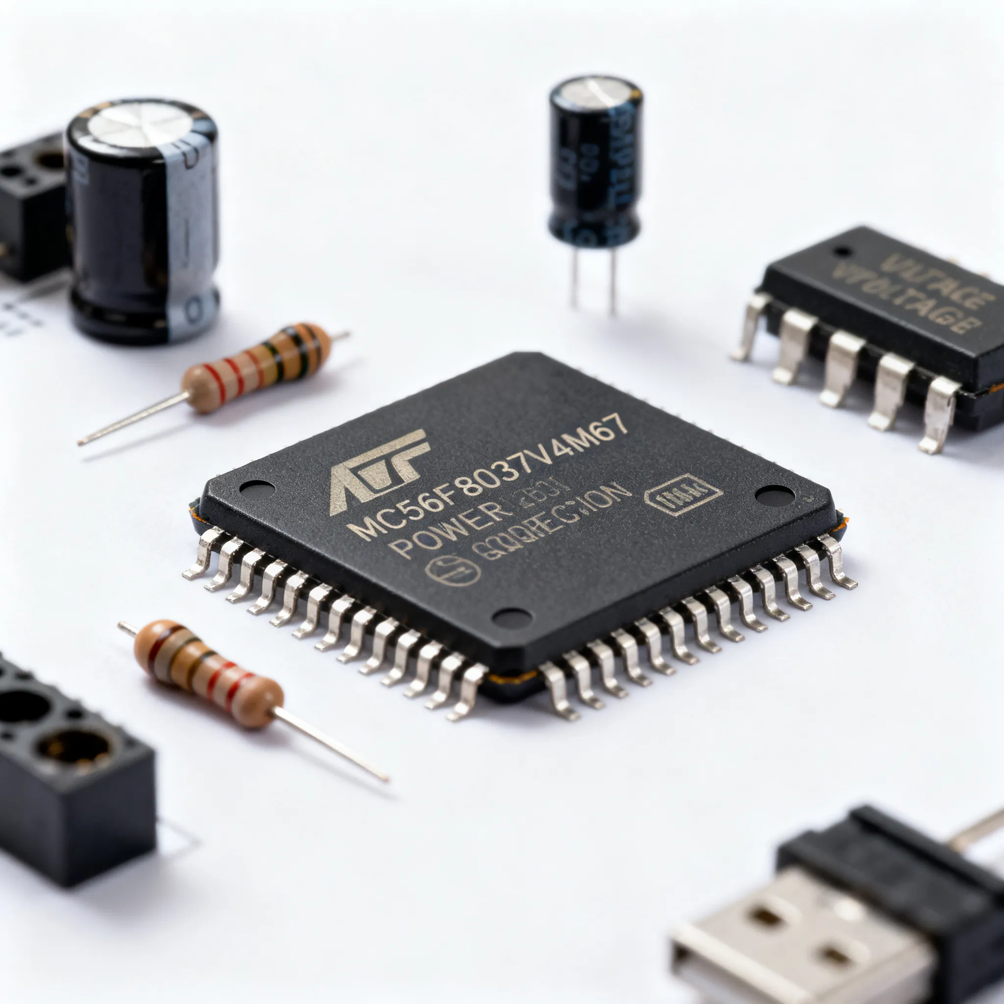
The Power-Up Lockup That Killed a Prototype: Why MC56F8037V4M67E Debugging Starts with Sequencing
When a prototype refuses to boot, engineers instinctively reach for the debugger, suspecting firmware bugs or clock configuration errors. Yet a growing body of field experience points to a more fundamental culprit: power sequencing. The MC56F8037V4M67E digital signal controller, with its multiple supply rails and sensitive flash memory, is particularly unforgiving of sloppy power-up behavior. Before you spend hours stepping through initialization code, ask yourself whether the silicon ever had a clean start.
Real-world failures on related NXP platforms illustrate the pattern. An S32K118 power-up lockup investigation documented how I/O pin voltage violations during the ramp phase can corrupt flash logic and force the device into a secured state, even when the firmware itself is flawless. Similarly, an IMX8MP PMIC failure thread on the NXP Community confirmed that connecting peripherals to processor I/O during power-up/down sequences can back-drive internal rails and trigger permanent damage. These aren’t isolated edge cases; they are the direct consequence of ignoring the power domain rules that the MC56F8037V4M67E inherits from the 56F8000 family architecture.
A general troubleshooting guide from ALLPCB reinforces this lesson: power-up integrity must be the first checkpoint in any microcontroller debug flow, not an afterthought. For the MC56F8037V4M67E, that means verifying that VDD and VDDA rise in the correct order, that ramp rates stay within datasheet limits, and that no external peripheral can inject voltage onto an I/O pin before the internal 1.8 V core regulator is stable. Skipping this step often leads to symptoms that masquerade as code bugs—random flash read errors, intermittent resets, or complete failure to exit reset—wasting days of engineering time.
Decoding the MC56F8037V4M67E Power Architecture: What the Datasheet Tells You About Sequencing
The MC56F8037V4M67E integrates a dual-supply architecture typical of mixed-signal DSP controllers. The digital core, I/O ring, and flash memory are powered from VDD, while the analog-to-digital converter and PLL analog blocks rely on VDDA. A common VSS/VSSA ground plane ties the domains together, but the separation of supply pins is not optional—it’s a hard requirement driven by internal isolation structures and the behavior of the on-chip voltage regulator that generates the 1.8 V core supply from VDD.
The MC56F8037 datasheet (Rev. 8) spells out the sequencing rules in unambiguous terms. VDD must reach its minimum operating level of 2.7 V before or simultaneously with VDDA. The ramp time from 0 V to 3.3 V should not exceed 100 ms, and the supply must be monotonic—no dips that could retrigger the power-on reset (POR) circuit. If VDDA leads VDD, the ADC reference and analog bias circuits can draw current through parasitic paths, pulling the digital supply into an indeterminate state. The result can be latch-up, flash initialization corruption, or a POR that releases before the internal regulator is fully settled.
The table below summarizes the critical power pins and their sequencing constraints. Ignoring these parameters is not a theoretical risk; it’s the most common root cause of “dead on arrival” prototypes in the 56F8000 family.
| Parameter | Value / Range | Unit / Notes |
|---|---|---|
| VDD (digital supply) | 3.0 – 3.6 | V; must reach ≥2.7 V before VDDA |
| VDDA (analog supply) | 3.0 – 3.6 | V; must not exceed VDD during ramp |
| VSS, VSSA (ground) | 0 | V; common plane, low impedance |
| Internal 1.8 V regulator output | 1.8 ± 10% | V; derived from VDD, not user-accessible |
| VDD ramp time (0→3.3 V) | ≤ 100 | ms; monotonic ramp required |
| VDDA ramp time | ≤ 100 | ms; must lag or equal VDD |
| I/O pin voltage during power-up | ≤ VDD + 0.3 | V; never exceed this limit |
| POR threshold (rising) | 2.3 – 2.7 | V; internal reset releases after this |
| LVD trip point | 2.7 – 2.9 | V; brown-out warning, not a sequencing fix |
Key takeaway: The on-chip POR and low-voltage detect (LVD) modules are designed to protect against brown-out events during steady-state operation, not to correct external sequencing errors. If VDDA rises before VDD, the internal bandgap reference may be biased incorrectly, and the POR circuit can release while the digital core is still in an unknown state. No amount of firmware delay can recover from a physically corrupted power-up sequence.
Debugging Power Sequencing on the MC56F8037V4M67E: Tools, Probes, and Simulation Trade-offs
Once you suspect a sequencing issue, the debug approach you choose determines how quickly you isolate the fault. Three distinct strategies have emerged in the embedded community, each with its own cost, visibility, and pre-silicon validation capability. The MC56F8037V4M67E supports standard JTAG/OnCE debug interfaces, but power rail behavior often occurs before the debugger can connect, making traditional run-control debugging blind to the critical first milliseconds.
Hardware probes that can sample analog voltages synchronously with the debug interface offer the most direct path to root cause. The SEGGER J-Link family, for example, can be paired with an external oscilloscope or logic analyzer to correlate power rail ramps with the moment the core exits reset. P&E Micro’s Multilink Universal FX provides real-time trace and can capture the exact cycle when the processor begins executing, helping you verify that the internal 1.8 V regulator settled before the first instruction fetch. Both approaches, however, require physical hardware and can only validate a board that already exists.
Power-aware simulation, discussed in detail by Electronic Design’s low-power debug pitfalls article, offers a complementary pre-silicon method. By modeling supply ramp behavior and power domain crossings, you can catch sequencing violations before layout. The Ignitarium SoC debug architecture guide highlights the inherent limitation: internal signal observability drops dramatically once the design moves to silicon, making simulation a valuable but incomplete safety net. Even complex SoCs like the Xilinx Zynq family face the same challenge, as the XC7Z010 vs XC7Z020 comparison notes—power sequencing issues remain a leading cause of board respins regardless of processor complexity.
The table below compares these three debug strategies for the MC56F8037V4M67E context.
| Comparison Metric | SEGGER J-Link + Scope | P&E Multilink Universal FX | Power-Aware Simulation |
|---|---|---|---|
| Power rail visibility | High (external scope required) | Medium (trace correlates with execution) | Full (any node in simulation) |
| Pre-silicon bug catching | No | No | Yes |
| Cost (approx.) | $400–$1,000 + scope | $249–$499 | Simulator license (varies) |
| Setup complexity | Moderate | Low | High (requires accurate models) |
| Real-time sequence capture | Yes, with trigger | Yes, cycle-accurate trace | No (simulated time only) |
| Best for | Post-layout validation | Firmware-hardware synchronization | Architecture and schematic review |
In practice, a layered approach works best. Use power-aware simulation during schematic design to verify that your external PMIC or supervisor enforces the VDD-before-VDDA rule. Then, on the first prototype, connect a J-Link or Multilink probe and trigger a scope on the VDD and VDDA rails while the debugger attempts to halt the core. If the core never reaches a stable state, you’ve confirmed a sequencing fault without writing a single line of test code.
From Schematic to Production: Avoiding Power Sequencing Pitfalls and Sourcing the Right MC56F8037 Variant
Designing a robust power tree for the MC56F8037V4M67E starts with a simple rule: never rely on the PCB trace inductance or an RC delay to sequence VDD and VDDA. A dedicated voltage supervisor or power management IC (PMIC) that provides a power-good signal and enforces a strict turn-on order is the only production-grade solution. The NXP IMX28CEC PMIC, while designed for the i.MX28 applications processor, illustrates the concept: it sequences multiple rails and holds off peripheral supplies until the core voltage is stable. For the MC56F8037V4M67E, a simpler dual-channel supervisor that monitors VDD and releases VDDA only after VDD exceeds 2.9 V eliminates the risk entirely.
Beyond the supply rails, pay attention to I/O pin behavior during power-up. Any peripheral that can drive a voltage onto an MCU pin before VDD is valid creates a back-drive path that can corrupt flash memory or trigger latch-up. The MPC5604P datasheet describes a flash fault collection unit (FCU) that reports errors even when the CPU is malfunctioning—a concept that applies equally to the 56F8000 flash controller. If an external sensor or communication IC powers up first and drives a logic high onto an unpowered MC56F8037V4M67E pin, the resulting current injection can flip bits in the flash array before the internal regulator reaches its nominal voltage.
Practical design rules to avoid these pitfalls:
- Insert series resistors (100 Ω to 1 kΩ) on all I/O lines that connect to independently powered peripherals. This limits injection current to safe levels during the brief window when the MCU is unpowered.
- Use bus switches or level translators with output enable pins tied to the MCU’s VDD rail. The switch should remain high-impedance until VDD crosses the POR threshold.
- Never connect a peripheral’s VCC to the same supply that powers VDDA unless you can guarantee the peripheral does not drive its outputs before the MCU is ready.
- Add a 10 µF low-ESR ceramic capacitor and a 100 nF bypass capacitor on each VDD/VDDA pin pair, placed as close as possible to the package. This minimizes voltage droop during inrush and keeps the ramp monotonic.
- If using an external watchdog or reset IC, configure its output to hold the MCU in reset until both VDD and VDDA are stable and within specification.
For procurement, the suffix “V4M67E” encodes critical ordering information that directly affects compatibility and reliability. The Kynix part number decoder provides a useful cross-reference, but you can break down the MC56F8037V4M67E identifier as follows:
| Suffix Element | Meaning | Impact on Sourcing |
|---|---|---|
| V | Temperature range: -40°C to +125°C | Industrial/automotive grade; do not substitute commercial range |
| 4M | Package: 64-pin LQFP (10×10 mm, 0.5 mm pitch) | Footprint-compatible only with other 64-LQFP 56F80xx variants |
| 67 | Speed grade and memory configuration | Indicates 32 MHz operation and specific flash/RAM size; verify against datasheet |
| E | RoHS compliance and lead finish | “E” suffix denotes lead-free, RoHS-compliant packaging |
When ordering, always purchase through authorized distributors such as Digi-Key, Mouser, or Newark. Counterfeit parts often have incorrect temperature grades or recycled packages that fail under thermal stress. Cross-check the full part number against the official NXP orderable part list to ensure you receive the exact variant your design requires.
MC56F8037V4M67E Power Sequencing and Debugging: Questions Engineers and Buyers Ask
Q: What is the exact power-up sequence for the MC56F8037V4M67E?
A: VDD (digital supply) must rise to at least 2.7 V before or simultaneously with VDDA (analog supply). The ramp time from 0 to 3.3 V should not exceed 100 ms. Violating this order can cause internal latch-up or corrupt flash initialization. The internal POR releases only after VDD crosses approximately 2.5 V, but the analog circuits require VDDA to be present within a few milliseconds of that event to ensure proper bias.
Q: Can I use a simple RC delay to sequence the power rails, or do I need a dedicated PMIC?
A: A simple RC delay is risky because it does not guarantee monotonic ramps or prevent reverse current from VDDA to VDD through internal ESD diodes. A dedicated PMIC or external voltage supervisor (e.g., a device with a power-good output that gates VDDA) that enforces proper sequencing and provides a clean reset signal is strongly recommended for production designs. The NXP IMX28CEC concept of sequenced power domains applies here: never leave sequencing to passive components.
Q: How do I prevent flash corruption when I/O pins are driven before VDD is stable?
A: Add series resistors (100 Ω–1 kΩ) on I/O lines that connect to external peripherals, and ensure peripherals are not powered before the MCU. Use level shifters or bus switches that disable outputs until VDD is valid. Never let an I/O pin voltage exceed VDD + 0.3 V during power-up. The flash array is particularly sensitive to injection current during the first few milliseconds; even a brief overvoltage can alter stored data.
Q: Are there known errata related to power sequencing on the MC56F8037?
A: Check NXP’s latest errata sheet for the specific mask set you are using. Common issues across the 56F8000 family include POR sensitivity to slow ramps (below 1 V/ms) and flash read errors if VDDA lags VDD by more than a few milliseconds. Always design with the worst-case ramp conditions from the datasheet, and verify the errata status of the flash controller and POR module before freezing the schematic.
Q: Where can I source authentic MC56F8037V4M67E parts and avoid counterfeits?
A: Purchase through authorized distributors (e.g., Digi-Key, Mouser, Newark) or directly from NXP franchised sources. Verify the full part number suffix “V4M67E” (64-LQFP, -40°C to +125°C) using the Kynix part number decoder or NXP’s own orderable part list to ensure you receive the correct variant and not a remarked or substandard part. Inspect incoming parts for consistent marking, proper date codes, and package integrity.
References & Further Reading
- Troubleshooting Common Microcontroller Issues in PCB Prototypes – ALLPCB
- S32K118 in Practice: Power-Up Lockups, CAN Fixes, and Hidden Tradeoffs – Kynix
- IMX8MP – PMIC Failure – NXP Community
- A Complete Guide to SoC Debugging | Part 1 – Ignitarium
- Solving Six Low-Power Debug Pitfalls – Electronic Design
- SEGGER Microcontroller GmbH Power-on Sequence – Farnell datasheet
- XC7Z010 vs XC7Z020: Entry-Level Zynq Comparison Guide – PCBSync
- MC56F8037/56F8027 Data Sheet, Rev. 8 – NXP
- IMX28CEC Data Sheet – NXP
- MPC5604P Data Sheet – NXP
- Professional Electronic Engineer, Electronic Information Blogs – Kynix (Part Number Decoder)
Power sequencing errors remain one of the most expensive and time-consuming debug challenges in embedded design. By treating the MC56F8037V4M67E power-up sequence as a critical design parameter—not a datasheet footnote—you eliminate the majority of flash corruption, latch-up, and mysterious reset failures before they reach the lab. Combine a disciplined hardware design with the right debug tools, and you’ll spend your time optimizing control algorithms instead of chasing phantom resets.
When you’re ready to move from prototype to production, sourcing authentic components with the exact suffix you need is just as important as the schematic itself. For mixed BOM procurement and flexible minimum order quantities, visit IC-Online to explore available inventory and connect with verified suppliers.