RF Module Integration Pitfalls: Antenna Matching, Power Supply Noise, and Layout Errors
Expert guide on RF Module Integration Pitfalls: Antenna Matching, Power Supply Noise, and Layout Errors. Technical specs, applications, sourcing tips for engineers and buyers.
Why RF Module Integration Failures Are Costing More Than the Module Itself
Pre‑certified RF modules promise to slash development time and sidestep the black art of radio design. The reality on the bench is often different. A $6 Bluetooth Low Energy module can trigger a $50,000 intentional‑radiator re‑test, a three‑month schedule slip, or a field‑failure rate that erodes a product’s reputation before the second production run. The root causes are rarely the module itself. They are the integration details that sit at the boundary between the module datasheet and the physical PCB: antenna matching, power‑supply noise, and layout parasitics.
Recent industry analysis from EE Times has underscored how the explosive growth of IoT devices is straining the supply of precision RF passives—high‑Q wirewound inductors, tight‑tolerance C0G capacitors, and miniature coaxial connectors. When a design team treats the module as a “drop‑in” black box and overlooks these passives, procurement inherits a BOM peppered with single‑source, long‑lead‑time components that can halt production. The integration pitfalls are not merely technical; they are strategic supply‑chain risks that demand joint attention from engineering and purchasing from the first schematic review.
This article maps the three most expensive integration traps—antenna mismatch, power‑rail noise, and layout errors—and provides practical, procurement‑aware guidance to keep your product on schedule and on budget.
How Antenna Mismatch, Power Rail Noise, and Layout Parasitics Undermine RF Performance
Every RF module is characterized on a pristine evaluation board with a perfect 50‑Ω load and a quiet bench supply. The moment you place that module on your own PCB, you introduce a cascade of small impairments that, individually, may seem negligible but together can push a link budget over the cliff. Understanding the physical mechanisms behind these losses is essential for reading between the lines of a datasheet and for writing a procurement specification that protects performance.
Impedance Mismatch and Return Loss
The antenna port of an RF module expects to see a well‑defined impedance, almost always 50 Ω. Any deviation reflects a portion of the transmitted power back into the module, quantified as return loss. A return loss of 10 dB (VSWR ≈ 2:1) means 10% of the power is reflected. That may sound acceptable, but in a low‑power link operating near sensitivity limits, a 3 dB drop in radiated power can halve the effective range. The matching network—typically a handful of capacitors and inductors—must compensate for the antenna’s inherent impedance, the PCB trace length, and parasitic reactances. Even a ±0.2 pF tolerance error in a 2.4 GHz matching capacitor can shift the resonant point enough to incur 2–3 dB of additional return loss.
Power Supply Noise Coupling
RF modules contain sensitive oscillators and low‑noise amplifiers. Noise on the supply rail couples into the VCO through the power‑supply rejection ratio (PSRR) of internal regulators, or directly into bias networks. A switching regulator that delivers 50 mV of ripple at 1 MHz can raise the phase noise floor of a 2.4 GHz carrier by 10 dB or more, degrading receiver selectivity and transmitter spectral mask compliance. Conducted noise also travels along the power trace and can radiate from the antenna structure, creating a self‑jamming scenario that no amount of matching can fix.
Layout Parasitics: The Invisible Circuit Elements
A 1 mm via stub on an antenna feed line behaves as an open‑circuit stub at 2.4 GHz, introducing a parallel reactance that can detune the antenna by 100 MHz. A ground plane that is pulled back too far under a chip antenna creates an asymmetric current distribution, distorting the radiation pattern and reducing gain. Long traces between the module’s RF pin and the antenna matching network add series inductance and loss—roughly 0.5 dB per centimeter on a typical FR‑4 substrate at 2.4 GHz. These layout‑dependent parasitics are not captured in the module vendor’s S‑parameter files, yet they dominate the final system performance.
| Pitfall | Typical Degradation | System Impact | Root Cause |
|---|---|---|---|
| Antenna impedance mismatch | 3 dB additional return loss | Range reduced by up to 50% | Matching component tolerance, trace length variation |
| Power supply ripple (50 mV) | 10 dB phase noise increase | Poor selectivity, spectral mask failure | DC‑DC converter noise, insufficient filtering |
| 1 mm via stub on antenna feed | 100 MHz frequency detuning | Link margin loss, certification failure | Unused via pad or layer transition stub |
| Insufficient ground clearance | 6–10 dB sensitivity loss | Shorter range, dead spots | Ground plane too close to antenna element |
| Long RF trace (2 cm) | 1 dB insertion loss | Reduced output power, higher current draw | Poor component placement, board stack‑up |
These numbers are not worst‑case outliers; they are routinely observed when a reference layout is not followed precisely. The next section helps you choose the antenna and filtering architecture that gives you the widest margin against these degradation mechanisms while keeping the BOM manageable.
Choosing the Right Antenna Topology and Filtering Strategy for Your RF Module
Antenna selection and power‑supply filtering are often treated as independent decisions, but they share a common thread: both directly affect the bill of materials, the procurement lead‑time profile, and the certification path. A poor antenna choice can force you into exotic matching components with 20‑week lead times, while an inadequate filtering strategy can demand last‑minute LDO swaps that ripple through the entire power tree.
Antenna Topology Trade‑offs
Chip antennas, PCB trace antennas, and external connectorized solutions each occupy a distinct corner of the cost‑performance‑size triangle. The table below captures the practical differences that matter to both the design engineer and the buyer.
| Comparison Metric | Chip Antenna (e.g., Johanson 2450AT18x100) | PCB Trace Antenna (Meandered Inverted‑F) | External Whip / Connectorized (U.FL / SMA) | Selection Criteria & Failure Boundary |
|---|---|---|---|---|
| Typical unit cost (10k volume) | $0.15–$0.40 | $0.00 (PCB copper) | $1.50–$4.00 (antenna + connector + cable) | PCB trace is free but consumes board area; external adds BOM lines and assembly steps. |
| Peak efficiency (2.4 GHz) | 50–65% | 55–70% | 70–85% | Efficiency below 50% can halve range; external antennas win when range is critical. |
| Sensitivity to enclosure proximity | High – detuning with plastic or metal within 5 mm | Moderate – can be tuned with keep‑out zone | Low – antenna can be placed away from enclosure | Enclosure‑induced detuning is a common field‑failure cause; factor in industrial design early. |
| Layout dependence | Requires precise ground‑plane clearance per datasheet | Requires exact trace dimensions; copied from reference | Minimal – only transmission line to connector matters | Even 1 mm deviation in clearance or trace width can shift resonance by 50–100 MHz. |
| Certification impact | Module grant usually covers same‑type antenna with equal or lower gain | Same as chip; must match reference design | Often triggers re‑certification if gain or type changes | Check module grant conditions; a different antenna type almost always requires intentional radiator re‑test. |
| Procurement lead‑time risk | 4–8 weeks; multiple sources available | None (PCB fab only) | Connectors (U.FL, MHF) can hit 16–30 weeks in shortages | Qualify second‑source connectors and cable assemblies during design, not after shortage hits. |
For many compact IoT products, a chip antenna offers the best balance of size and repeatability, provided the layout follows the vendor’s keep‑out zone exactly. When range is paramount and the industrial design permits, an external antenna with a U.FL connector gives the highest efficiency but introduces a mechanical connection that must meet IPC Class 2 or 3 reliability standards for shock and vibration. The connector itself becomes a critical procurement item; miniature RF connectors from suppliers like I‑PEX and Hirose have historically experienced allocation during periods of high demand.
Power Supply Filtering: Passive, Ferrite, or Active?
Noise on the supply rail is just as damaging as antenna mismatch, yet the filtering strategy is often an afterthought. The table below compares the three most common approaches, incorporating the component tolerance and lead‑time factors that procurement teams must manage.
| Filtering Approach | Typical Parts | Noise Attenuation (100 MHz / 1 GHz) | Component Tolerance & Lead‑Time Risk | Cost & BOM Impact |
|---|---|---|---|---|
| Passive LC filter (single‑stage) | 10 µH inductor + 10 µF capacitor | 20–30 dB / 10–15 dB | High‑Q wirewound inductors (e.g., Murata LQW series) can have ±5% tolerance and 16‑week lead times; C0G capacitors ±0.1 pF are stable but tight‑tolerance values may be single‑source. | Low component cost ($0.05–$0.20) but may need multiple stages for wideband suppression. |
| Ferrite bead + capacitor | Murata BLM18 series bead + 10 µF MLCC | 25–35 dB at 100 MHz (bead impedance peak) / 5–10 dB at 1 GHz | Bead impedance curve varies with DC bias and temperature; select bead with R (resistive) characteristic at target frequency. Lead times typically 8–12 weeks; second‑source from TDK or Taiyo Yuden. | Very low cost ($0.02–$0.10); small footprint; effective for narrowband noise. |
| Active low‑noise LDO | Analog Devices ADP150, TI TPS7A20 | 40–60 dB PSRR up to 1 MHz; 20–30 dB at 1 GHz (with external bypass) | LDOs are active components with 12–20 week lead times during shortages; tolerance is specified as PSRR and noise spectral density. Always qualify a pin‑compatible second source. | Higher cost ($0.30–$0.80) but provides clean rail for entire RF section; reduces passive count. |
The ferrite bead approach is popular because it is cheap and compact, but its effectiveness hinges on selecting a bead whose impedance is predominantly resistive at the noise frequency, not inductive. A bead that looks inductive at 100 MHz can form a resonant tank with the bypass capacitor, creating a noise peak instead of suppressing it. Active LDOs offer the highest PSRR at low frequencies but need careful layout to maintain stability. From a procurement standpoint, the passive LC filter carries the greatest risk of single‑source bottlenecks on precision inductors; early qualification of alternate footprints (e.g., 0402 vs. 0201) and second‑source vendors is a must.
Design and Procurement Tactics to Avoid the Most Common RF Integration Traps
Armed with an understanding of the failure mechanisms and the trade‑offs between topologies, you can now embed resilience into both the design and the supply chain. The following tactics are field‑proven and address the intersection of engineering and procurement.
Specify capacitor dielectrics explicitly. For antenna matching and RF filtering, C0G (NP0) capacitors are non‑negotiable. They exhibit negligible capacitance change with temperature and voltage, unlike X7R or X5R dielectrics that can lose 50% of their rated capacitance under DC bias. A matching network built with X7R capacitors will drift with temperature and applied power, degrading return loss. Write the procurement specification to require C0G dielectric and a tolerance of ±0.1 pF or ±0.25 pF for values below 10 pF. Multiple vendors (Murata, TDK, AVX) supply these parts, but the tightest tolerances can narrow the supply base—qualify at least two sources during the design phase.
Select ferrite beads by their R‑vs‑frequency curve, not just impedance. A bead’s impedance magnitude at 100 MHz tells only half the story. The resistive component (R) dissipates noise as heat; the inductive component (X) stores energy and can resonate. For power‑rail filtering, choose a bead whose impedance is predominantly resistive in the frequency band of your switching noise. Consult the manufacturer’s impedance‑vs‑frequency charts and derate for DC bias current, which can reduce the bead’s effective impedance. Second‑source beads from TDK and Taiyo Yuden that exhibit similar R‑X characteristics to avoid a redesign if one vendor goes on allocation.
Enforce keep‑out zones and via stitching per IPC‑2221 guidelines. The module vendor’s reference layout is not a suggestion; it is a tested, certified configuration. Any deviation—moving a ground via, shrinking a keep‑out area, or routing a digital trace through the antenna clearance—can introduce 6–10 dB of sensitivity loss. Use the IPC‑2221 standard as a baseline for RF transmission line design and grounding. Stitch the ground plane with vias along the RF trace at intervals no greater than λ/20 (about 3 mm at 2.4 GHz) to suppress parallel‑plate modes and reduce radiation from the ground return path.
Qualify alternative passive components early. High‑Q wirewound inductors (e.g., for matching networks) and tight‑tolerance capacitors are often the first parts to go on allocation during a market upswing. During the prototyping phase, identify pin‑compatible alternates in different case sizes (e.g., 0402 and 0201) and from different manufacturers. Build a procurement specification that captures the critical parameters—inductor Q at the operating frequency, self‑resonant frequency (SRF), and DC resistance—without locking in a single vendor part number. This gives the purchasing team the flexibility to switch sources without a design change notice.
Engage the module vendor’s layout review service. Most reputable module suppliers (Nordic, Silicon Labs, u‑blox, TI) offer a layout review as part of their design support. Use it. The review catches subtle mistakes—like a missing ground via under the module’s thermal pad or a trace routed too close to the antenna matching network—that can take weeks to debug in the lab. Schedule the review before freezing the PCB layout, and share the Gerber files along with the stack‑up information. This step alone can prevent the majority of integration‑related certification failures.
Monitor supply‑chain intelligence continuously. The lead‑time landscape for RF passives and connectors can shift in weeks. Subscribe to distributor alerts and keep an eye on market analysis from EE Times and industry associations. When a connector like the U.FL or MHF series shows signs of tightening, have the alternate part number already approved in the AVL. Procurement should also consider holding buffer stock of the most critical, long‑lead‑time passives, especially if the product is ramping to volume.
RF Module Integration: Questions Engineers and Buyers Should Ask Before Finalizing a BOM
Q: What tolerance is really needed for antenna matching capacitors and inductors?
For narrowband matching at 2.4 GHz, a tolerance of ±0.1 pF for capacitors below 2 pF and ±0.2 nH for inductors below 5 nH is typical. A 0.2 pF error can shift the resonant frequency by 50–100 MHz, causing a 2–3 dB increase in return loss. Always use C0G capacitors, which maintain their value over temperature and voltage, and wirewound inductors with high Q and tight tolerance. Buyers should secure at least two qualified sources for these precision parts; single‑source risk on a ±0.1 pF capacitor can delay the entire production ramp.
Q: How can I verify power supply noise without an anechoic chamber?
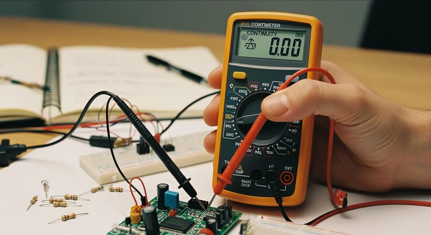
Conducted noise on the power rail can be measured with a spectrum analyzer and a high‑impedance near‑field probe placed directly on the supply trace. Set the analyzer to the frequency band of interest and measure the ripple before and after adding filtering. For a relative radiated‑noise figure of merit, use a simple TEM cell or a calibrated antenna in a semi‑shielded environment (even a large metal box with absorber can suffice). The key is to correlate the conducted noise spectrum with the module vendor’s conducted emissions data and to confirm that the noise floor drops by the expected amount when filtering is applied.
Q: If I use a pre‑certified module, do antenna changes force re‑certification?
Yes, in most regulatory domains (FCC, CE). A modular certification grant typically permits antenna changes only if the new antenna is of the same type (e.g., PCB trace to PCB trace) and has equal or lesser gain. Switching from a chip antenna to an external whip, or even lengthening the trace to the connector, alters the radiated emissions profile and requires intentional radiator re‑testing. Always check the module’s grant conditions—often published in the FCC ID database or the vendor’s certification notes—and involve an accredited test lab early to avoid a costly schedule slip.
Q: What are the lead‑time risks for RF‑specific passives and connectors?
High‑Q wirewound inductors, tight‑tolerance C0G capacitors, and miniature RF connectors (U.FL, MHF series) have historically experienced lead times of 16–30 weeks during market shortages. Procurement should qualify alternate footprints (e.g., 0402 vs. 0201) and second‑source parts during the design phase, not after the shortage hits. Monitoring market intelligence from EE Times and distributor supply‑chain alerts helps anticipate tightening conditions. For connectors, pre‑negotiated buffer stock agreements with distributors can prevent line‑down situations.
Q: What PCB layout details most often degrade module performance?
The most common layout errors are: insufficient ground‑plane clearance under the antenna, long traces between the module’s RF pin and the antenna matching network, missing via stitching along the RF transmission line, and placement of noisy digital lines (e.g., SPI, I2C) near the antenna or the power input. Following IPC‑2221 design guidelines and the module vendor’s reference layout exactly is essential. Even a 1 mm deviation in the antenna keep‑out zone can cause a 6–10 dB sensitivity loss that is difficult to diagnose without an anechoic chamber.
Q: Should I buy modules with an integrated antenna or use an external connector?
Integrated antennas (chip or PCB trace) simplify design and certification, but they limit range and are sensitive to enclosure materials and nearby components. External antennas offer higher gain and placement flexibility but add connector cost, mechanical integration complexity, and potential re‑certification. The decision should be driven by the product’s range requirements, industrial design constraints, and the procurement team’s ability to manage connector and cable supply. If the product must operate through a metal enclosure or at ranges beyond 50 meters, an external antenna is usually the better choice, provided the supply chain for the connector and cable assembly is secured.
Navigating these pitfalls requires a tight partnership between engineering and procurement. By treating the integration as a strategic risk and embedding supply‑chain resilience into the design from the start, you can avoid the hidden costs that turn a cost‑effective RF module into an expensive liability. For teams sourcing mixed BOMs with flexible minimum order quantities, IC-Online provides a streamlined platform to secure the precision passives, connectors, and modules your design demands without over‑committing inventory.
References & Further Reading
- EE Times – Electronics Engineering News – Industry analysis on IoT connectivity and component supply chains.
- IPC Standards – IPC‑2221 design guidelines and IPC‑A‑610 assembly standards for RF hardware.
- Murata Inductor Product Line – High‑Q wirewound inductors and ferrite beads for RF matching and filtering.
- TDK Ferrite Bead Application Guide – Impedance vs. frequency characteristics and DC bias derating.
- Analog Devices ADP150 Low‑Noise LDO – Example of an active supply‑noise solution for RF modules.
- Texas Instruments TPS7A20 Low‑Dropout Regulator – Alternative low‑noise LDO with high PSRR.
- Johanson Technology – Chip antenna and RF passive component datasheets and layout guidelines.
- IC-Online – Mixed BOM procurement with flexible MOQ for RF passives, connectors, and modules.