IGBT Symbol Quick Reference: Pin Identification and Practical Selection for Power Designs
Expert guide on IGBT Symbol Quick Reference: Pin Identification and Practical Selection for Power Designs. Technical specs, applications, sourcing tips for engineers and buyers.
Why Misreading an IGBT Symbol Can Cost You a Power Stage
Every power electronics engineer has stared at a schematic symbol and assumed it was “just another MOSFET.” That assumption is especially dangerous when the device is an insulated-gate bipolar transistor (IGBT). The IGBT schematic symbol closely mimics a power MOSFET—gate, collector/drain, emitter/source—but the subtle differences carry heavy consequences. A designer who drops a generic MOSFET symbol into a motor-drive schematic can easily misroute the gate drive, swap collector and emitter, or overlook the co‑packaged freewheeling diode. The result is often a board respin, a blown gate driver, or a power stage that self-destructs during the first hard‑switching test.
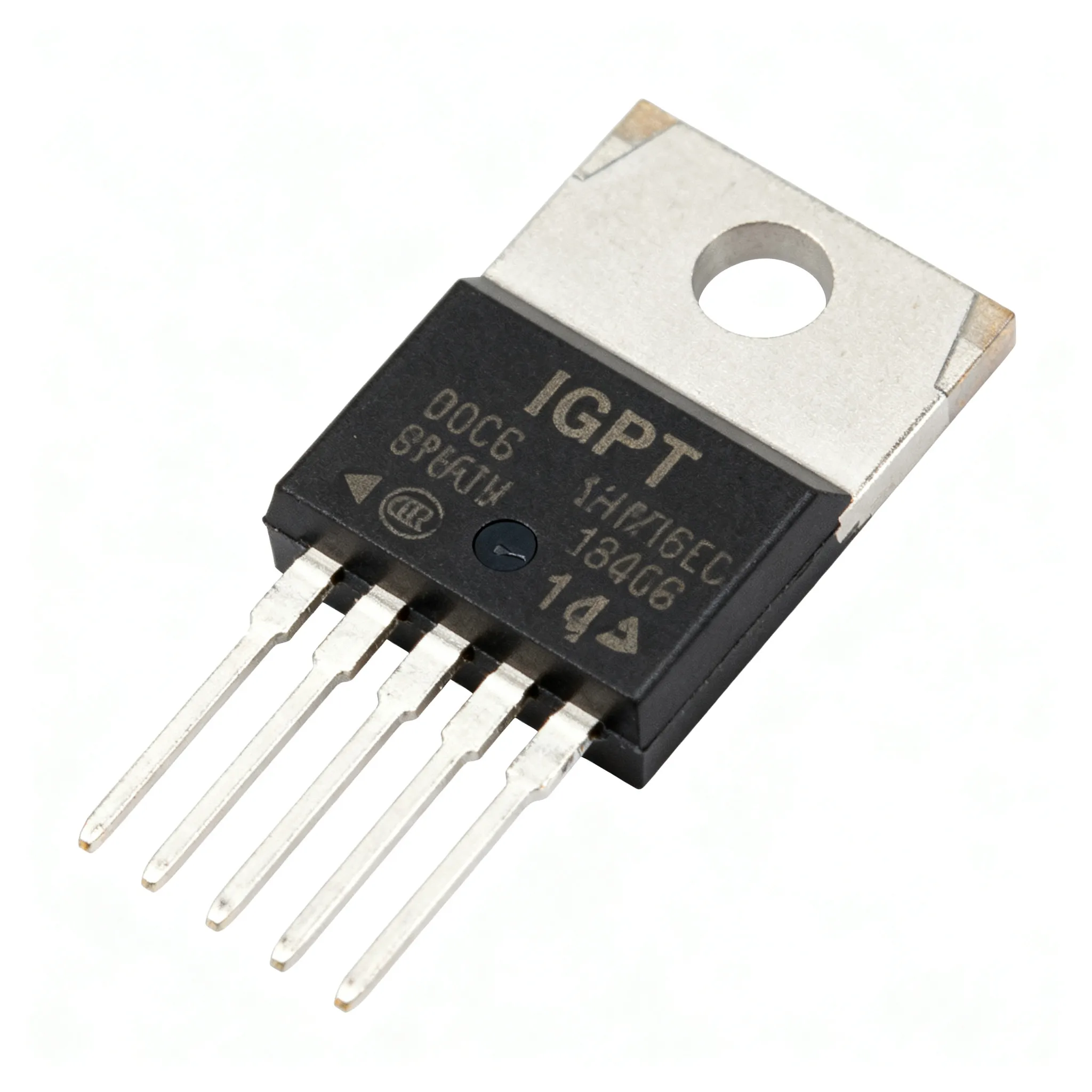
The most common trap is pin misidentification. The schematic symbol shows a gate on the left, a collector at the top, and an emitter at the bottom, but the physical pinout of a TO‑247 or TO‑220 package rarely follows that visual order. Even experienced engineers have placed a gate‑drive trace on pin 2 of a TO‑247, only to discover that the tab—and pin 2—is the collector, floating at the high‑voltage rail. This kind of error is not caught by a DRC; it shows up as a short circuit when the bus voltage is applied.
Another costly oversight is ignoring the symbol’s built‑in anti‑parallel diode. In a half‑bridge inverter, the diode conducts the freewheeling current. If the schematic symbol omits the diode (or the designer uses a symbol without one), the layout may lack a low‑inductance return path, causing voltage overshoots that exceed the device’s breakdown rating. Reference guides for schematic symbols from IEC/ANSI standards emphasize that the IGBT symbol is distinguished by a thicker collector‑emitter line and a diode symbol across those terminals—details that are absent in a standard MOSFET symbol. Misreading these cues can turn a 50‑cent part into a $5,000 field failure.
Finally, the gate terminal itself deserves respect. The IGBT gate is insulated by a thin silicon oxide layer, exactly like a MOSFET gate. This oxide creates an input capacitance that must be charged and discharged by the gate driver, and it is just as vulnerable to electrostatic discharge. The Toshiba IGBT application note explains that the gate oxide’s capacitance directly influences switching speed and drive requirements. A schematic that treats the gate as a simple logic input, without accounting for gate charge and Miller plateau, will produce slow switching, excessive losses, or unintended shoot‑through. The symbol alone doesn’t convey these realities; only a disciplined pin‑identification and selection process can bridge the gap between a clean schematic and a working power stage.
Decoding the IGBT Schematic Symbol: Gate, Collector, Emitter, and the Body Diode
At first glance, an IGBT symbol looks like an N‑channel MOSFET with an extra junction. The gate is drawn as a vertical line separated from the channel region, the collector is the top terminal, and the emitter is the bottom terminal with an arrow. The key visual cues that distinguish it from a MOSFET are the thicker line representing the collector‑emitter path and the diode symbol connected anti‑parallel between collector and emitter. These additions reflect the IGBT’s hybrid nature: a MOSFET‑controlled gate driving a bipolar PNP transistor output, with a body diode often integrated into the same die or co‑packaged.
The arrow on the emitter follows BJT convention, not MOSFET convention. For an N‑channel IGBT—the overwhelming majority in power designs—the arrow points out of the emitter, indicating the direction of electron flow. This is opposite to the arrow on an N‑channel MOSFET, which points from the body to the source. The difference is subtle but critical when interpreting a symbol from an unfamiliar library. Comprehensive schematic symbol references note that the IGBT symbol is “similar to MOSFET but with thicker load line and diode symbol,” and this thicker line is the fastest way to spot an IGBT on a crowded schematic.
The table below maps each symbol element to its physical pin and function, providing a quick reference that you can use when auditing a schematic or building a footprint.
| Symbol Element | Physical Pin | Function | Key Characteristics |
|---|---|---|---|
| Gate (G) | Pin 1 (typical discrete) | Voltage‑controlled input; turns the device on/off | Insulated by thin silicon oxide; input capacitance Cies dominates gate drive requirements (Toshiba app note) |
| Collector (C) | Tab and/or pin 2 (TO‑247/TO‑220) | High‑side power terminal; connects to the PNP collector | Thick line in symbol indicates high‑current path; often tied to the heatsink tab |
| Emitter (E) | Pin 3 (typical discrete) | Low‑side power terminal; reference for gate voltage | Arrow points out for N‑channel; carries both MOSFET channel current and bipolar collector current |
| Anti‑parallel diode | Between collector and emitter (internal or co‑packaged) | Freewheeling path for inductive loads | Not present in all IGBTs; when shown, it’s a separate diode symbol across C‑E. Check reverse recovery charge Qrr |
The gate’s insulation is a double‑edged sword. While it provides high input impedance and easy voltage control, the thin oxide layer is sensitive to overvoltage and ESD. The Toshiba application note reminds us that “the gate is insulated by a thin silicon oxide. Therefore, an IGBT has capacitances” that dictate the gate charge curve. A gate driver must source and sink peak currents that can exceed several amperes to charge the input capacitance quickly, even though the steady‑state gate current is near zero. The symbol gives no hint of this dynamic behavior, which is why pin identification must always be paired with a thorough datasheet review.
IEC vs. ANSI IGBT Symbols and Package Pinouts: What Changes on Your Schematic
IGBT symbols vary slightly between IEC and ANSI drawing standards, but both conventions preserve the essential elements: an insulated gate, a collector‑emitter path with a thicker line, and an optional anti‑parallel diode. In IEC schematics, the gate is often drawn as a single vertical line with no bubble, while ANSI symbols may add a small circle to indicate logic inversion—though this is less common for IGBTs than for MOSFETs. The real schematic‑to‑layout disconnect, however, has nothing to do with drawing style. It’s the physical pin order that trips up designers, because the symbol’s left‑to‑right or top‑to‑bottom arrangement rarely matches the package pin numbering.
A TO‑247 IGBT typically has the gate on pin 1, the collector on the metal tab (which is also pin 2), and the emitter on pin 3. A TO‑220 follows the same pattern. But there are exceptions: some devices swap gate and emitter, and modules often include a Kelvin emitter sense pin that does not appear on the basic three‑terminal symbol. Schematic symbol guidelines emphasize that you must “always match symbol to actual package pinout in the datasheet.” The symbol is a functional abstraction, not a wiring diagram.
The table below compares common discrete IGBT packages and their standard pin assignments. Use it as a sanity check when transitioning from schematic capture to PCB layout.
| Package | Pin 1 | Pin 2 / Tab | Pin 3 | Notes |
|---|---|---|---|---|
| TO‑247 | Gate | Collector (tab) | Emitter | Most common high‑power discrete package. Some variants add a Kelvin emitter on pin 4 (4‑lead TO‑247). Always verify. |
| TO‑220 | Gate | Collector (tab) | Emitter | Widely used up to ~100 A. Pin order identical to TO‑247 but smaller footprint. |
| TO‑3P / TO‑264 | Gate | Collector (tab) | Emitter | Larger package for higher current; pin order consistent with TO‑247. |
| SOT‑227 (miniBLOC) | Gate (pin 1) | Collector (pin 2, tab) | Emitter (pin 3) | Isolated baseplate; screw terminals. Often used in industrial modules. Check for auxiliary emitter pins. |
| ISOTOP / SOT‑227 module | Gate (pin 4 or 5) | Collector (power screw) | Emitter (power screw) | Pin numbering varies by manufacturer. Auxiliary emitter for gate drive return is common. |
The takeaway is clear: the schematic symbol tells you which terminal is the gate, collector, and emitter, but it never reveals the physical pin number. When you place a TO‑247 symbol on a schematic, the gate pin might be on the left, but on the board it’s pin 1, which could be the rightmost pad depending on your footprint orientation. For modules with Kelvin emitter connections, the symbol may show only three terminals, leaving the sense pin undocumented. In these cases, you must create a custom symbol or add a separate test point to avoid floating the gate‑drive return. Procurement teams should also note that the same IGBT die may be available in multiple packages with different pinouts—a detail easily missed when a BOM lists only the generic part number.
From Symbol to Layout: Practical Pin Identification and Selection Rules for IGBTs
Bridging the gap between a schematic symbol and a reliable power layout requires a disciplined, repeatable workflow. The following steps have been refined across hundreds of inverter, converter, and motor‑drive designs, and they apply whether you are selecting a 600‑V discrete IGBT for a PFC stage or a 1.7‑kV module for a traction drive.
- Match the symbol to the manufacturer’s datasheet pinout first. Before placing a single trace, open the datasheet for the exact part number and locate the pin configuration diagram. Compare it to the schematic symbol you are using. If the symbol shows the gate on the left but the datasheet shows pin 1 as the emitter, redraw the symbol or swap the pin mapping in your CAD library. Never assume a standard pin order.
- Identify any Kelvin emitter or auxiliary connections. Many medium‑ and high‑power IGBT modules include a separate emitter sense pin that provides a clean reference for the gate driver, bypassing the inductive voltage drops in the main emitter path. The basic three‑terminal symbol will not show this pin. Check the datasheet for a “Kelvin emitter” or “auxiliary emitter” terminal and add it to your schematic as a separate net, typically tied to the gate driver’s return.
- Verify gate threshold voltage and saturation voltage under real load conditions. The gate threshold voltage VGE(th) tells you the minimum gate voltage needed to begin conduction, but it is specified at a tiny collector current (often 250 µA). For hard‑switching applications, you need to drive the gate well beyond the threshold—typically to +15 V—to ensure the IGBT is fully saturated. The collector‑emitter saturation voltage VCE(sat) is a strong function of collector current and junction temperature. STMicroelectronics’ IGBT datasheet tutorial explains how to interpret VCE(sat) curves and how they shift with gate voltage and temperature. A device that looks good on the front page may have excessive conduction losses at your operating current if you don’t check these curves.
- Evaluate switching energies and diode recovery. Turn‑on and turn‑off energy (Eon, Eoff) are specified at a given collector current, gate resistance, and temperature. These values directly determine switching losses. Equally important is the anti‑parallel diode’s reverse recovery charge Qrr, which causes a current spike during turn‑on of the complementary switch. Bourns’ guide to IGBT data sheet parameters walks through these dynamic characteristics and shows how to estimate total power dissipation. In hard‑switched topologies, a diode with excessive Qrr can force you to add an external SiC Schottky diode, increasing cost and board area.
- Match the load type to the IGBT rating. The Toshiba application note highlights that “the specified parameters and their conditions differ between resistive and inductive loads.” An IGBT rated for 40 A resistive may only handle 30 A inductive at the same case temperature because of the higher switching losses and the diode’s contribution. Always check the safe operating area (SOA) for both forward bias and reverse bias, and derate according to your maximum junction temperature.
To make the selection process concrete, the table below lists the critical datasheet parameters you must verify for any IGBT, along with typical ranges for a 600‑V, 40‑A discrete device and the reason each matters.
| Parameter | Symbol | Typical Range (600 V, 40 A) | Why It Matters |
|---|---|---|---|
| Collector‑emitter saturation voltage | VCE(sat) | 1.5 – 2.5 V at IC = 40 A, Tj = 25°C | Determines conduction losses; increases with temperature, so check at Tj(max) |
| Gate threshold voltage | VGE(th) | 4.0 – 6.5 V | Minimum gate voltage for turn‑on; dictates logic‑level compatibility and noise margin |
| Total gate charge | Qg | 50 – 200 nC at VGE = 15 V | Directly sets gate drive current requirement and switching speed |
| Turn‑on energy | Eon | 0.5 – 2.0 mJ (at Rg = 10 Ω, inductive load) | Switching loss per cycle; scales with frequency |
| Turn‑off energy | Eoff | 0.3 – 1.5 mJ | Tail current contributes to turn‑off loss; critical in hard‑switched circuits |
| Diode reverse recovery charge | Qrr | 0.5 – 5 µC | Causes turn‑on current spike; high Qrr may require external fast diode |
| Thermal resistance (junction‑to‑case) | RthJC | 0.3 – 0.8 °C/W | Used with power loss to calculate junction temperature rise |
| Safe operating area (forward bias) | FBSOA | Square‑shaped up to 2× rated current at 1 ms | Ensures device survives start‑up and fault transients |
When you combine this parameter checklist with the pin‑identification steps above, you create a selection process that is both fast and robust. Procurement professionals can use the same table to qualify alternative sources: if a second‑source IGBT matches these parameters within acceptable margins, it is likely a drop‑in replacement. However, always re‑verify the package pinout—even within the same manufacturer’s portfolio, a TO‑247 device may have a different pin assignment than a TO‑3P version of the same die.
IGBT Pin Identification and Selection: Questions from the Lab Bench
Q: How can I quickly tell the gate pin on an IGBT symbol when it looks almost identical to a MOSFET?
A: Look for two visual cues that a MOSFET symbol lacks: the thicker line between collector and emitter, and the diode symbol pointing from emitter to collector. The gate is the isolated terminal on the left side, drawn with a vertical line separated from the channel region—exactly like a MOSFET gate. However, the symbol’s left‑right order does not correspond to physical pin numbering. In a TO‑247, the gate is pin 1, but on the schematic it may appear anywhere. Always cross‑reference the datasheet pinout diagram before assigning footprints.
Q: Does every IGBT symbol include a freewheeling diode, and what if my circuit doesn’t need it?
A: Not every IGBT includes a diode. Many discrete IGBTs are co‑packaged with an anti‑parallel diode, and the symbol will show a diode across the collector‑emitter terminals. If the symbol omits the diode, the device has no internal diode. Even when a diode is present, you must check its reverse recovery characteristics. In hard‑switched applications such as motor drives, the internal diode’s Qrr may be too high, forcing you to add an external fast‑recovery or SiC Schottky diode. The symbol alone does not convey the diode’s performance; always consult the datasheet’s dynamic characteristics section.
Q: Why does the arrow on the IGBT emitter point outward, and does it indicate N‑channel or P‑channel?
A: The arrow direction follows bipolar junction transistor convention, not MOSFET convention. For an N‑channel IGBT—the standard type in power electronics—the arrow points out of the emitter, indicating the direction of electron flow from emitter to collector (conventional current flows from collector to emitter). A P‑channel IGBT would have the arrow pointing inward, but these are exceedingly rare in high‑power designs because of their inferior carrier mobility and higher on‑state losses. If you encounter an IGBT symbol with an inward‑pointing arrow, double‑check that it is not a mis‑drawn N‑channel MOSFET.
Q: I’m using a TO‑247 IGBT. Is the collector always the tab, and how do I identify the gate and emitter without a symbol?
A: In standard TO‑247 packages, the metal tab is the collector, pin 1 is the gate, and pin 2 is the emitter. However, this is a convention, not a guarantee. Some manufacturers swap gate and emitter, and 4‑lead TO‑247 packages use pin 3 for the emitter and pin 4 for a Kelvin emitter sense. Without a symbol, you must locate the part number on the device and download the datasheet. The pinout diagram is usually on the first page. Never rely on a generic footprint library or a visual inspection of the die—misidentifying the gate can destroy the device instantly.
Q: What are the most critical datasheet parameters to verify beyond the symbol when selecting an IGBT?
A: Beyond the symbol, focus on five groups of parameters: (1) conduction: VCE(sat) at your operating current and maximum junction temperature; (2) gate drive: VGE(th), total gate charge Qg, and internal gate resistance; (3) switching: Eon and Eoff at your target gate resistance and voltage; (4) diode: Qrr and reverse recovery energy; (5) thermal: RthJC and the safe operating area. STMicroelectronics’ IGBT datasheet tutorial provides a detailed walk‑through of each parameter, and Bourns’ understanding IGBT data sheet parameters explains how to interpret the graphs. Always match the load type—inductive or resistive—because the ratings differ significantly.
When you’re ready to move from symbol decoding to procurement, IC-Online’s IGBT category gives you access to a wide range of discrete and module IGBTs from leading manufacturers, with flexible MOQs and real‑time availability. Whether you need a standard TO‑247 for a PFC stage or a 1.7‑kV module for an industrial drive, starting with a correct pin‑identification process ensures that the part you order is the part you actually place on the board.
References & Further Reading
- IGBTs (Insulated Gate Bipolar Transistor) Application Note – Toshiba
- IGBT Datasheet Tutorial – STMicroelectronics
- Understanding IGBT Data Sheet Parameters – Bourns
- Comprehensive Schematic Symbols Reference: IEC & ANSI Guide – SchematicsHub
- IGBT Products – Infineon Technologies
- IGBT Power Transistors – STMicroelectronics
- IGBT – Toshiba Electronic Devices & Storage
- Insulated‑Gate Bipolar Transistor – Wikipedia
- IGBT Transistors – Digi‑Key Electronics
- IGBT Category – IC-Online