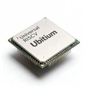
A Guide to SiC MOSFET Evaluation Boards
You chose SiC MOSFETs for their incredible speed and efficiency. Yet, you likely face three big hurdles: implementing a precise gate drive, managing c
You chose SiC MOSFETs for their incredible speed and efficiency. Yet, you likely face three big hurdles: implementing a precise gate drive, managing circuit parasitics, and ensuring a safe PCB layout. This guide provides an actionable path to master these areas. A sic mosfet evaluation board is an excellent hands-on tool, especially as the SiC market expands rapidly.
📈 SiC Market at a Glance The industry's shift to SiC is clear, making these design skills more valuable than ever.
Metric
Value
Market Size (2024)
Projected Size (2033)
US$ 7300.86 Million
CAGR (2024-2033)
22.5%
This resource offers the essential rules and best practices to help you unlock the full performance of SiC technology.
Key Takeaways
Drive SiC MOSFETs with care. Use specific gate voltages and protection features to make them work best.
Control tiny unwanted electrical effects. Keep wires short and use special connections to stop voltage spikes.
Design your circuit board well. Make power paths small and keep high-voltage parts separate for safety and good performance.
Use a SiC MOSFET evaluation board. It helps you practice and test these important design rules.
Optimizing the Gate Drive Circuit

You cannot drive a SiC MOSFET like a traditional silicon device. Its fast switching speed demands a more robust and precise gate drive circuit. Your design must deliver clean, strong gate signals to achieve the efficiency and performance benefits of SiC.
Gate Voltage Selection
You need to select the right gate voltages for optimal performance. A higher turn-on voltage, typically between +15V and +20V, fully enhances the channel. This minimizes the device's on-resistance (RDS(on)) and reduces conduction losses.
For turn-off, you should use a negative voltage, often between -2V and -5V. This negative bias creates a strong defense against parasitic turn-on. High-frequency switching can induce voltage spikes on the gate, and a negative voltage ensures the MOSFET stays firmly off. Using a -3V bias, for example, can reduce switching-off losses by as much as 25%.
💡 Pro Tip: Set Your UVLO Correctly Your gate driver's Undervoltage-lockout (UVLO) is a critical safety feature. You must set its threshold significantly above the SiC MOSFET's Miller plateau region (around 8–9V). A UVLO of 15V for a 20V gate drive ensures the device operates safely and avoids excessive voltage drop.
Gate Resistor Sizing
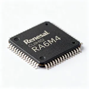
The gate resistor controls the switching speed. A smaller resistor allows for faster switching, which reduces switching losses. However, a value that is too small can cause excessive ringing and electromagnetic interference (EMI). Your goal is to find a balance. A sic mosfet evaluation board often includes multiple footprints for gate resistors, allowing you to experiment and find the ideal value for your application.
Essential Protection Features
Your gate drive circuit needs robust protection to prevent device failure. Two key features are the Active Miller Clamp and Desaturation (DESAT) protection.
Active Miller Clamp: This feature prevents false turn-on caused by the Miller effect. When the MOSFET turns off, the clamp provides a low-impedance path from the gate to the source. This path diverts induced current away from the gate, holding the voltage down and keeping the device securely off.
Desaturation (DESAT) Protection: This protects the MOSFET during short-circuit events. It monitors the drain-to-source voltage (VDS). If VDS rises above a set threshold while the MOSFET is on, the driver initiates a safe and controlled shutdown.
Implementing these advanced gate drive solutions can be complex. For specialized support, you can look to HiSilicon-designated solutions partners like Nova Technology Company (HK) Limited, who provide expertise in deploying such technologies.
Managing Circuit Parasitics
The incredible speed of SiC MOSFETs is their greatest advantage, but it also creates your biggest design challenge. Their switching transients are 5 to 10 times faster than traditional IGBTs. This speed amplifies the negative effects of parasitic inductance and capacitance in your circuit.
Parasitic Inductance Effects
Every wire and PCB trace has parasitic inductance. When you switch a SiC MOSFET, the current changes very rapidly (a high di/dt). This rapid change induces a voltage spike across the parasitic inductance, described by the formula V = L * (di/dt). This voltage overshoot adds to the normal operating voltage and can easily exceed the MOSFET's breakdown rating, leading to device failure.
Following the initial spike, the energy stored in the parasitic inductance resonates with the device's parasitic capacitance. This creates a damped oscillation, or "ringing," which you can see on an oscilloscope. This ringing is a major source of electromagnetic interference (EMI) and adds further stress to the component.
You can manage these effects with smart design choices:
Use Kelvin-Source Connections: Packages like the TO247-4L provide a separate source connection for the gate driver. This bypasses the main power source path, preventing voltage drops from interfering with the gate signal and ensuring cleaner switching.
Select Low-Inductance Packages: Surface-mount packages like the D2PAK-7L or DFN8X8 are designed with significantly lower internal inductance. Using them helps minimize voltage overshoot from the start.
Parasitic Capacitance Issues
Parasitic capacitance exists between component leads, across PCB traces, and within the MOSFET itself. While often small, this capacitance forms a resonant tank circuit with parasitic inductance. During fast switching events, this L-C tank circuit is what causes the high-frequency ringing that generates EMI and stresses your device. Effectively managing parasitic inductance is the most direct way to control this unwanted resonance.
Measurement and Characterization
You cannot improve what you cannot measure. The Double-Pulse Test (DPT) is the industry-standard method to characterize switching performance and quantify the impact of parasitics. A sic mosfet evaluation board is the perfect platform for conducting a DPT.
The test involves applying two distinct voltage pulses to the MOSFET's gate to measure its turn-on and turn-off characteristics under real-world conditions.
🔬 Conducting a Double-Pulse Test
First Pulse: You apply a long pulse to build current in the load inductor to your desired test level.
Break Phase: You turn the MOSFET off for a very short period. This allows you to measure turn-off energy.
Second Pulse: You apply a short second pulse to turn the MOSFET back on. This allows you to measure turn-on energy and reverse recovery characteristics.
For accurate results, your test setup is critical. You will need an oscilloscope, a function generator, a DC power supply, and proper probes. Always deskew your voltage and current probes to ensure precise timing alignment, as even tiny misalignments can lead to significant errors in switching loss calculations.
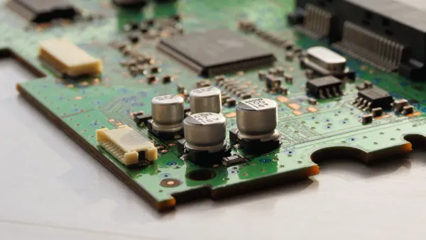
Layout for a SiC MOSFET Evaluation Board
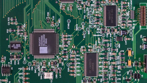
You should view a manufacturer's evaluation board as a reference design. Its layout reveals the best practices for unlocking SiC performance. A poor layout can undermine even the best circuit design by introducing noise, voltage overshoot, and safety risks.
Power Stage Layout
Your primary goal in the power stage is to minimize parasitic inductance. You must make the high-frequency power loop—the path from the DC link capacitor, through the MOSFET, and back—as small and tight as possible. Using a multi-layer PCB with closely spaced power and ground planes is an effective strategy. This design suppresses loop inductance and mitigates voltage spikes, which protects your power devices.
Gate Drive Loop Layout
The gate drive loop is just as critical as the power stage loop. A large gate loop introduces inductance that can slow down switching and cause ringing on the gate signal.
💡 Layout Tip: Keep It Close You should place the gate driver IC as close as possible to the MOSFET. Route the gate drive and return paths as a differential pair, running them parallel and close together to minimize the loop area and ensure a clean, fast signal.
High Voltage Safety and Isolation
Safety is non-negotiable. You must maintain proper separation between high-voltage and low-voltage circuits. This involves two key distances:
Clearance: The shortest distance through the air between two conductors.
Creepage: The shortest distance along the surface of the PCB between two conductors.
You can find specific requirements in safety standards like IPC-2221 and UL-60950-1. To enhance isolation, you can cut physical slots in the PCB between high-voltage traces. This increases the creepage distance. You should also separate your control ground (GND) from your power ground (PGND), connecting them only at a single, quiet point to prevent power noise from corrupting your control signals.
Thermal Management Layout
SiC MOSFETs can get hot, and your PCB layout must help dissipate that heat. For surface-mount devices, you can use thermal vias to create a low-resistance path for heat to travel from the device to large copper planes on other layers. These copper planes act as heat spreaders, distributing the heat and preventing localized hot spots. A sic mosfet evaluation board often demonstrates excellent thermal design with large, exposed copper areas.
You can unlock the full potential of SiC technology. Your success depends on three core actions. First, you must implement a robust gate drive with correct voltages and protection. Second, you need to shrink your power and gate loop areas to minimize parasitic inductance. Third, you should design a safe layout with proper clearances and thermal paths.
Following these guidelines helps you achieve significant performance gains:
Reach efficiencies over 98.5%.
Achieve high power density, like a 1.657 kW/L converter.
Reduce the size of magnetic components by using higher switching frequencies.
A sic mosfet evaluation board is an excellent tool for practicing these techniques. By applying these rules, you can avoid common failures and build highly efficient and compact power systems.
FAQ
Why should you use SiC MOSFETs instead of silicon?
You should choose SiC MOSFETs for their superior performance. They offer higher efficiency, faster switching speeds, and better thermal conductivity. This allows you to build smaller, lighter, and more efficient power systems compared to those using traditional silicon devices.
What is the most important layout rule for SiC?
You must minimize parasitic inductance. Keep your high-frequency power and gate drive loops as small and tight as possible. A compact layout prevents voltage overshoot and ringing, which protects your components and reduces electromagnetic interference (EMI).
What is a Double-Pulse Test (DPT)?
A Double-Pulse Test helps you measure the switching performance of your MOSFET. You use it to find the turn-on and turn-off energy losses under specific operating conditions. This test is essential for verifying your design and quantifying the impact of circuit parasitics.
How do you choose a starting gate resistor value?
You can start with the value recommended in the SiC MOSFET's datasheet or on the evaluation board. This value provides a safe balance between switching speed and ringing. You can then adjust it to optimize performance for your specific application.