HiSilicon AI SoCs A Guide to BOM and Reference Designs
Obtaining a reference design and BOM for a project begins with a key choice. Engineers first select a specific SoC model, li
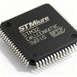
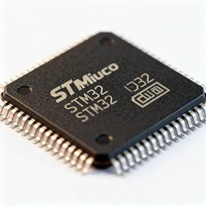
Obtaining a reference design and BOM for a project begins with a key choice. Engineers first select a specific SoC model, like the Hi3516DV300, based on project needs. The official Hardware Development Kit, or 开发套件, contains the schematics and layout files. This 半导体开发套件 is available from HiSilicon or its distributors. HiSilicon AI SoCs lead the global market with powerful and efficient AI. The company's NPU-powered chip technology drives countless smart devices.
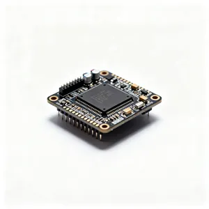
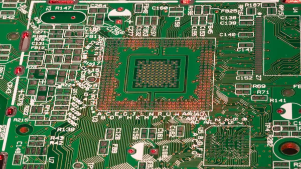
Core Component Focus: The reference design focuses on the main pcb. The pcb must support the primary chip and a memory chip. This pcb connects every chip. The pcb layout for the main chip is critical. A good pcb ensures the chip performs well. The pcb and chip function as one system. The pcb needs a quality chip. The pcb design supports the main ic. This 套件 simplifies pcb and chip integration.
Key Takeaways
- Choose the right HiSilicon AI chip for your project. Match its AI power to your needs.
- Study the reference design. It shows how to connect the main chip and manage its power.
- Design the PCB carefully. A good PCB helps the chip work well and prevents problems.
- Build a Bill of Materials (BOM). This list helps you choose parts and manage costs.
- Check component availability. Make sure you can get all parts for your product.
SELECTING HISILICON AI SOCS
Selecting the right chip is the first step in designing an effective product. Engineers must map project requirements to the capabilities of specific HiSilicon AI SoCs. This process ensures the final device performs as expected. A well-chosen chip simplifies the PCB design and integration.
MAPPING COMPUTE POWER TO SOCS
AI compute power is measured in Tera Operations Per Second (TOPS). A higher TOPS rating means the chip can handle more complex AI tasks. This is a critical factor for any ML project.
- Hi3516DV300: Offers up to 1.0 TOPS, suitable for entry-level AI analytics.
- Hi3559AV100: Provides 2.0 TOPS, ideal for more demanding AI applications.
The NPU, or Neural Processing Unit, is the core of the AI capability. The Kirin 970 chip, with its dedicated NPU, shows a 7-21 times speed-up on certain AI tasks compared to its CPU. This performance boost is vital for real-time processing. The PCB layout must support the power and data needs of this powerful integrated circuit. A good PCB design ensures the chip operates at peak efficiency.
MATCHING AI FEATURES TO USE CASE
Different applications require different HiSilicon AI SoCs. The choice of chip directly impacts the final product's features.
Use Case Examples:
- Multi-Channel Surveillance: The Hi3536 chip is an excellent choice for NVRs, supporting up to 128 channels for intelligent video analysis.
- High-Accuracy Facial Recognition: A chip with strong AI performance, like those in the Smart Vision Platform, is necessary. These systems can search a 50,000-face database in under 300ms.
- Entry-Level Smart Home: The Hi3516AV200 is a cost-effective hardware solution for basic motion detection. This 嵌入式解决方案 is perfect for affordable devices.
ANALYZING KEY HARDWARE SPECS
Engineers must also analyze key hardware specifications. These specs determine the device's core functions and affect the PCB design. The main IC and its supporting components on the PCB define the system. The PCB connects the chip to memory, power, and peripherals like the 传感器.
Key specs include video encoding, interfaces, and power. For example, the Hi3519A chip supports 4K@60fps H.265 encoding. Power consumption is also crucial. The Hi3559A chip consumes around 2.6 Watts, a key detail for the thermal design of the PCB. This 半导体 chip requires careful PCB planning. The 嵌入式 system's stability depends on a quality PCB that manages heat and signal integrity for the main chip and each connected 传感器. The PCB is the foundation that allows the chip to function.
ANALYZING THE REFERENCE DESIGN

The reference design is the official blueprint for a product. Engineers use this guide to understand the hardware architecture of HiSilicon AI SoCs. It shows how to connect the main chip to all other components. A careful analysis of this design is the foundation for building a stable and high-performing device. The design provides a proven starting point, which saves significant development time.
CORE SOC AND POWER SUBSYSTEM
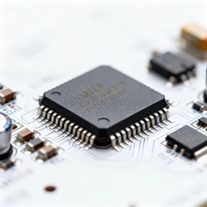
The core of the reference design centers on the main chip and its power system. This integrated circuit contains the CPU, the NPU for AI tasks, and the Image Signal Processor (ISP). These units work together to process data. The system requires a stable and clean power source to function correctly.
Power Delivery Network (PDN): The power delivery network is a critical part of the design. It ensures every part of the chip receives the correct voltage. A well-designed PDN prevents system crashes and performance issues.
The Power Management IC, or 电源管理ic, is a key component. This special IC takes a single input voltage, like 5V or 12V, and converts it into multiple different voltages. The main chip needs these specific voltages for its various internal blocks. The primary 电源 system relies on the 电源管理ic to regulate power efficiently. The reference design specifies the exact 电源管理ic and shows how to lay out the connections on the PCB. A crystal oscillator also provides a stable clock signal, which acts as the heartbeat for the entire chip.
CORE PCB LAYOUT CONSIDERATIONS
The layout of the printed circuit boards, or PCB, is extremely important. The PCB connects all electronic components. A poor PCB layout can cause a powerful chip to fail. The reference design provides a complete PCB layout file. Engineers study this file to learn best practices for their own custom PCB.
Key considerations for the PCB layout include:
- High-Speed Signal Integrity: Signals for DDR memory and MIPI interfaces travel at very high speeds. The PCB traces for these signals must have specific lengths and spacing. This prevents data corruption. The PCB design ensures the chip communicates reliably with memory.
- Thermal Management: The main chip generates heat during operation. The PCB helps dissipate this heat. The layout often includes thermal vias and large copper planes under the chip. These features transfer heat away from the 半导体 device, preventing it from overheating.
- Power Plane Design: The PCB uses dedicated layers, called power planes, to distribute the main 电源. This approach provides a low-noise power source to the chip. A clean power supply is essential for stable AI and ML processing.
This 嵌入式 system's performance depends heavily on the quality of the PCB. The PCB is not just a board; it is an engineered component that enables the chip to perform at its peak.
MEMORY AND PERIPHERAL INTERFACES
The reference design details how to connect the chip to memory, storage, and other peripherals. These connections define the product's features and capabilities. The PCB layout must carefully route these connections.
| Interface Type | Component | Purpose on the PCB |
|---|---|---|
| Memory | DDR4 SDRAM | Provides fast, volatile memory for the CPU and NPU to run applications. |
| Boot Storage | SPI NOR Flash | Stores the initial bootloader. The chip reads from it on startup. |
| Main Storage | eMMC Flash | Offers reliable, non-volatile storage for the operating system and user data. |
| Image Input | MIPI CSI-2 | Connects a camera 传感器 to the chip's ISP for image capture. |
| Network | Ethernet PHY | An external IC that enables a wired network connection. |
| Audio | Audio Codec | An external IC that processes audio input from a microphone or output to a speaker. |
Engineers must choose the right components for their 嵌入式解决方案. For example, a device needing fast boot times will use SPI NOR flash. The MIPI CSI-2 interface is standard for connecting a high-resolution camera 传感器. The PCB must have clean routing for the 传感器 data lines to ensure image quality. The reference design shows the correct way to implement these interfaces, from the physical connections on the PCB to the selection of the external ICs. This ensures compatibility and reliable operation of every connected 传感器.
BUILDING THE PRODUCTION BOM
After analyzing the reference design, engineers move to a critical phase: building the production Bill of Materials (BOM). This process transforms the reference blueprint into a manufacturable and cost-effective product. A well-managed bom is essential for a successful production run. It directly impacts the final cost, assembly process, and supply chain stability of the device.
EXTRACTING THE BASE BOM
The journey begins with the official Hardware Development Kit (开发套件). This kit contains a complete list of every component used in the reference design. Engineers extract this list to create their initial bom. This base document includes manufacturer part numbers, component descriptions, and quantities needed for a single printed circuit boards assembly. It serves as the foundational checklist for the entire project. The quality of the final pcb depends on the accuracy of this initial list.
Note: The reference BOM is a starting point, not the final destination. It is optimized for performance and validation, not always for cost. Engineers must review every line item.
COST OPTIMIZATION STRATEGIES
Reducing production cost is a primary goal for any commercial product. Engineers carefully analyze the BOM to find savings without sacrificing quality. This optimization focuses on both high-cost and high-volume components. The pcb design itself can influence these costs.
Key high-cost items often include:
- The main HiSilicon AI chip.
- DDR memory chips.
- The high-resolution image 传感器.
While the main chip is usually fixed, engineers can find savings elsewhere. They can source pin-compatible passive components like resistors and capacitors from different vendors. This strategy lowers cost without changing the pcb layout. For active components, engineers balance cost and performance. A cheaper Ethernet PHY ic might save money, but it could have higher power consumption, affecting the pcb thermal design. The main 电源 system also offers optimization opportunities. Choosing a more integrated 电源 management chip can reduce the component count on the pcb. Every decision impacts the final pcb assembly cost. A smart choice for one chip can simplify the entire pcb.
| Component Category | Optimization Tactic | Impact on PCB |
|---|---|---|
| Main SoC | Fixed choice based on performance needs. | The central component defining the pcb footprint. |
| DDR Memory | Source from multiple approved vendors. | No change if pin-compatible. |
| Passive Components | Find lower-cost, pin-compatible alternatives. | No change to the pcb layout. |
| Power Management | Balance cost vs. efficiency for the main 电源. | May require minor pcb adjustments. |
| Connectors | Select cost-effective but reliable options. | Footprint must match the pcb design. |
SUPPLY CHAIN AND LIFECYCLE MANAGEMENT
A successful 嵌入式 product requires a stable supply of components. Engineers must manage the supply chain to avoid production delays. This involves checking the lifecycle status of every part on the BOM.
Lifecycle Status Check: ⚠️ Engineers must verify that components are not marked as "Not Recommended for New Designs" (NRND) or "End of Life" (EOL). Using an EOL chip or 传感器 could halt production entirely.
Identifying second-source options is a critical strategy. For many components, multiple manufacturers produce compatible parts. Having an alternative supplier for a critical chip protects the project from shortages. This is especially important for memory, power components, and connectors. Even the primary 半导体 chip may have different packaging options that require pcb layout variants. A robust supply chain plan considers these factors from the beginning. Engineers work with distributors to secure volume pricing and forecast demand. This ensures the components for the pcb are available when needed for mass production. A well-planned supply chain is the backbone of a scalable hardware product, from the main chip to the smallest resistor on the pcb.
Engineers build successful products with Hisilicon AI SoCs by following a clear workflow. They select a chip for the required AI performance, analyze the reference design for pcb needs, and then optimize the production bom. This process ensures a stable pcb. The final pcb design is the foundation for the entire system. The quality of the printed circuit boards and the main chip determines the success of any AI project. A good pcb supports the chip's AI functions.
Final Project Checklist: ✅
- Confirm the AI TOPS requirement for your pcb.
- Verify sensor compatibility with the pcb layout.
- Identify second-source options for the main chip to ensure pcb assembly is not delayed. The pcb footprint must match.
FAQ
Where do I find the official PCB layout files?
Engineers find official layout files in the Hardware Development Kit (HDK). These files provide the complete pcb design. They show the correct pcb layout for high-speed signals. A good pcb is essential. The reference pcb ensures stability. This pcb is a proven starting point.
Can I change components from the reference BOM?
Yes, engineers can change components. A different component might need a pcb layout change. The new part's footprint must match the pcb. This ensures the pcb assembly is successful. Engineers must verify compatibility to maintain performance.
Why is the PCB layout so important for the SoC?
The pcb layout is critical for performance. It manages heat from the chip. A quality pcb prevents signal issues. The pcb connects all components reliably. A poor pcb can cause the entire system to fail, even with a powerful chip.