The 2025 Guide to a Modern PCB Board Fix
A successful pcb board fix involves a clear process. This troubleshooting process includes finding the fault, prep
A successful pcb board fix involves a clear process. This troubleshooting process includes finding the fault, preparing tools, and executing a precise repair. This guide demystifies pcb troubleshooting for the growing electronics community.
The DIY tools market is a growing field. Projections estimate its value will reach USD 973.34 billion by 2025.
Good troubleshooting helps locate issues on a printed circuit board. It is the key to creating effective solutions for any pcb circuit. This guide provides solutions for common pcb issues, from a broken circuit trace on a pcb to a faulty component on the circuit board.
Key Takeaways
- Always start with a visual check. Look for cracks, burns, or corrosion on the PCB. This helps find many common problems.
- Use a multimeter to test connections. It helps find breaks or shorts that you cannot see. A schematic diagram guides this process.
- Gather the right tools before you start. A soldering iron, desoldering pump, and safety gear are important. This prevents more damage and keeps you safe.
- Fix cracked traces with a jumper wire or copper tape. Re-secure lifted pads with epoxy. These steps restore the electrical path.
- Replace faulty parts carefully. Use a vacuum desoldering tool for through-hole parts. A hot air station works best for small surface-mount parts.
PCB Troubleshooting: Finding the Fault

An excellent PCB troubleshooting process is the foundation of any successful repair. Before picking up a soldering iron, a technician must first become a detective. This phase focuses on identifying the exact location and nature of the fault. A multimeter and a schematic are the primary tools for finding non-physical issues, such as an open circuit. However, many problems can be found with just a careful look. This systematic approach to troubleshooting ensures that the repair is targeted and effective.
Visual Inspection: What to Look For
The first step in any pcb troubleshooting process is a thorough visual check. Many common pcb issues are visible to the naked eye, especially with good lighting and magnification. A technician should clean the pcb with isopropyl alcohol to remove any dust or residue that might hide problems.
Look for obvious signs of damage first. These include physical cracks, burn marks from overheating, or signs of corrosion from water damage. Discolored or sticky areas often point to old flux residue or electrical arcing, which can cause future issues. Pay close attention to solder joints for these common defects:
- Solder Bridging: An unwanted connection between two points that creates a short circuit.
- Tombstoning: A component lifts at one end, creating an open circuit.
- Solder Balls: Tiny spheres of solder that can cause shorts if they move.
- Insufficient Solder: Weak or missing joints that lead to an open circuit.
Testing with a Multimeter
A multimeter is essential for diagnosing issues that are not visible. It helps confirm continuity and find short circuits. For effective pcb troubleshooting, set the multimeter to continuity mode, often marked with a sound wave symbol.
To check for an open circuit, place the multimeter probes on two points of a trace that should be connected. A beep or a reading near zero ohms confirms the connection is good. No beep indicates a break in the circuit. To find a short circuit, test two adjacent traces that should be separate. A beep in this case signals a short. This simple troubleshooting technique is powerful for verifying the electrical integrity of a pcb. Testing components like diodes is also straightforward. In diode test mode, a good diode should show a voltage drop (e.g., 0.5V-0.8V) in one direction and an open line (OL) when the probes are reversed.
Using Schematics for Diagnosis
A schematic diagram is a roadmap for a pcb. It makes the pcb troubleshooting process much faster. If a schematic is available, use it to understand the intended circuit path. Start by identifying the power (VCC) and ground (GND) connections. Follow the signal path from inputs to outputs, using reference designators like R1 (resistor) or C1 (capacitor) to locate components on the circuit board.
Use the multimeter in continuity mode to trace connections on the pcb and verify they match the schematic. This helps pinpoint breaks or shorts with high precision. Many online resources, like Build-Electronic-Circuits.com and HobbyProjects.com, offer schematics for common electronics, which can be a great help for troubleshooting.
Intro to PCB Reverse Engineering
What happens when there is no schematic? This is where pcb reverse engineering comes in. PCB reverse engineering is the process of recreating a pcb layout and schematic from a physical board. For simple, single or double-layer boards, this reverse engineering process is quite manageable for hobbyists. The goal is to create a new schematic by analyzing the existing pcb.
The basic steps of pcb reverse engineering involve taking high-resolution photos of the pcb, tracing the connections, and identifying each component. Software like KiCad or EasyEDA can then be used to draw the schematic and recreate the layout. While complex, multi-layer boards often require professional services, understanding the fundamentals of pcb reverse engineering is a valuable addition to one's troubleshooting skills. The advantages of pcb reverse engineering include the ability to repair obsolete electronics. The applications of pcb reverse engineering extend to improving or modifying existing designs. This troubleshooting approach turns a black box into an understandable circuit.
Safety and Prep: Your Repair Toolkit
Successful pcb troubleshooting requires more than just knowledge. A technician needs the right tools and a safe workspace. Proper preparation prevents further damage to the pcb and ensures personal safety. This phase bridges the gap between finding the fault and fixing it.
Essential Soldering and Desoldering Tools
A good toolkit is the foundation of any pcb repair. A technician should gather these items before starting any work.
- A soldering station with temperature control
- Desoldering pumps or solder wicks
- Solder wire and flux
- A multimeter for testing
- Wire strippers and screwdrivers
For most hobbyists, a simple soldering iron is enough for basic tasks. However, a hot air station offers more precision for modern pcb work, especially with small surface-mount components. It heats parts without direct contact, reducing the risk of damage.
| Feature | Hot Air Soldering Station | Soldering Iron |
|---|---|---|
| Heat Source | Hot air stream | Heated metal tip |
| Application | SMD rework, chip removal | Through-hole, basic assembly |
| Contact | Non-contact | Direct contact |
| Cost | Higher | Lower |
Specialized Repair Materials
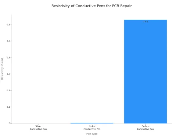
Sometimes a repair needs more than just solder. Specialized materials help fix physical damage to the pcb itself. For a broken trace, a conductive pen offers a quick fix. These pens use silver, nickel, or carbon ink to redraw a conductive path.
For lifted pads, a two-part epoxy is the industry-standard solution. A technician applies the epoxy to bond the new pad securely to the pcb surface.
Tip: Never use regular super glue for pad repair. It cannot withstand soldering temperatures and will fail.
Critical ESD and Fume Safety Gear
Safety should always be the top priority in electronics work. Electrostatic discharge (ESD) can instantly destroy sensitive components on a pcb. Industry standards like ANSI/ESD S20.20 exist to prevent this. A technician must use an ESD wrist strap and an anti-static mat to protect the pcb.
Solder fumes also pose a health risk. These fumes contain irritants that can cause headaches and respiratory issues. An effective fume extractor is not optional; it is essential for safe pcb troubleshooting and repair. It captures harmful particles at the source, creating a safer work environment.
Executing Your PCB Board Fix
With the fault identified, the next phase is the hands-on pcb board fix. This is where a technician applies skill and precision to restore the pcb to working order. Each type of damage requires a specific technique. Following the correct procedure is critical for a lasting repair and preventing new issues. This part of the troubleshooting process provides solutions for the most common pcb problems.
Repairing a Cracked PCB Trace
A cracked trace creates an open circuit, stopping signals from flowing. The repair method depends on the size of the break. A technician can use a jumper wire or conductive copper tape to fix these issues.
For larger breaks, a jumper wire is a reliable solution. This pcb board fix restores the electrical path. The process is straightforward:
- Inspect and Clean: A technician first finds the break using a multimeter. He or she then cleans the area with isopropyl alcohol to remove any dirt.
- Expose Copper: The solder mask covering the trace must be removed. A technician carefully scrapes away about 2-3 mm of the mask on both sides of the break to expose the copper.
- Prepare the Jumper: A small piece of 30 AWG wire is cut to length. The ends are stripped and tinned with a small amount of solder.
- Solder the Wire: The technician solders one end of the wire to the exposed copper on one side of the break. He or she then solders the other end to the opposite side, bridging the gap.
- Protect the Repair: A layer of solder mask or epoxy is applied over the repair. This protects the exposed wire from corrosion and shorts.
- Test the Connection: The final troubleshooting step is to test the pcb for continuity to ensure the circuit is complete.
For smaller breaks or quick fixes, copper foil tape offers an excellent alternative. It has several advantages for pcb troubleshooting.
- Fast Repairs: The tape allows for quick fixes. A technician just cuts, sticks, and solders the tape in place.
- Excellent Conductivity: It is made of pure copper and ensures a low-resistance connection, matching the original circuit performance.
- Flexible and Safe: The tape can be cut to fit any pcb layout. It carries less risk of creating accidental shorts compared to a loose wire.
Fixing Lifted Pads and Through-Holes
Pads and through-holes are critical connection points on a pcb. Excessive heat or mechanical stress can cause them to lift or break, creating serious issues.
For a lifted pad that is still attached to its trace, a technician can re-secure it using epoxy. This technique is for pads that are not completely detached. The goal is to bond the pad back to the pcb surface. A two-part epoxy is carefully applied under the lifted pad. The pad is pressed down, and the epoxy is allowed to cure. This creates a strong mechanical bond.
Important: A technician should never use standard super glue for this repair. It cannot handle soldering temperatures and will fail, causing more issues for the pcb.
For a damaged plated through-hole, a more robust solution is needed. Using small metal eyelets is an industry-standard method that conforms to IPC guidelines. This technique restores the integrity of the circuit connection.
- Clean the area around the damaged hole on the pcb.
- Select an eyelet that matches the component lead and board thickness.
- Insert the eyelet into the hole.
- Use a special setting tool to flare the eyelet barrel, securing it to the pcb.
- Apply flux and solder the eyelet to any connecting traces on the circuit board.
- Perform a final troubleshooting check for electrical continuity.
Choosing the right eyelet is key for a successful pcb board fix.
| Criteria | Description |
|---|---|
| ID (Inside Diameter) | Must be slightly larger than the component lead. |
| OD (Outside Diameter) | Should be smaller than or equal to the original hole diameter. |
| LUF (Length Under Flange) | Must be equal to or slightly less than the pcb thickness. |
| FD (Flange Diameter) | Should be smaller than or equal to the original pad diameter. |
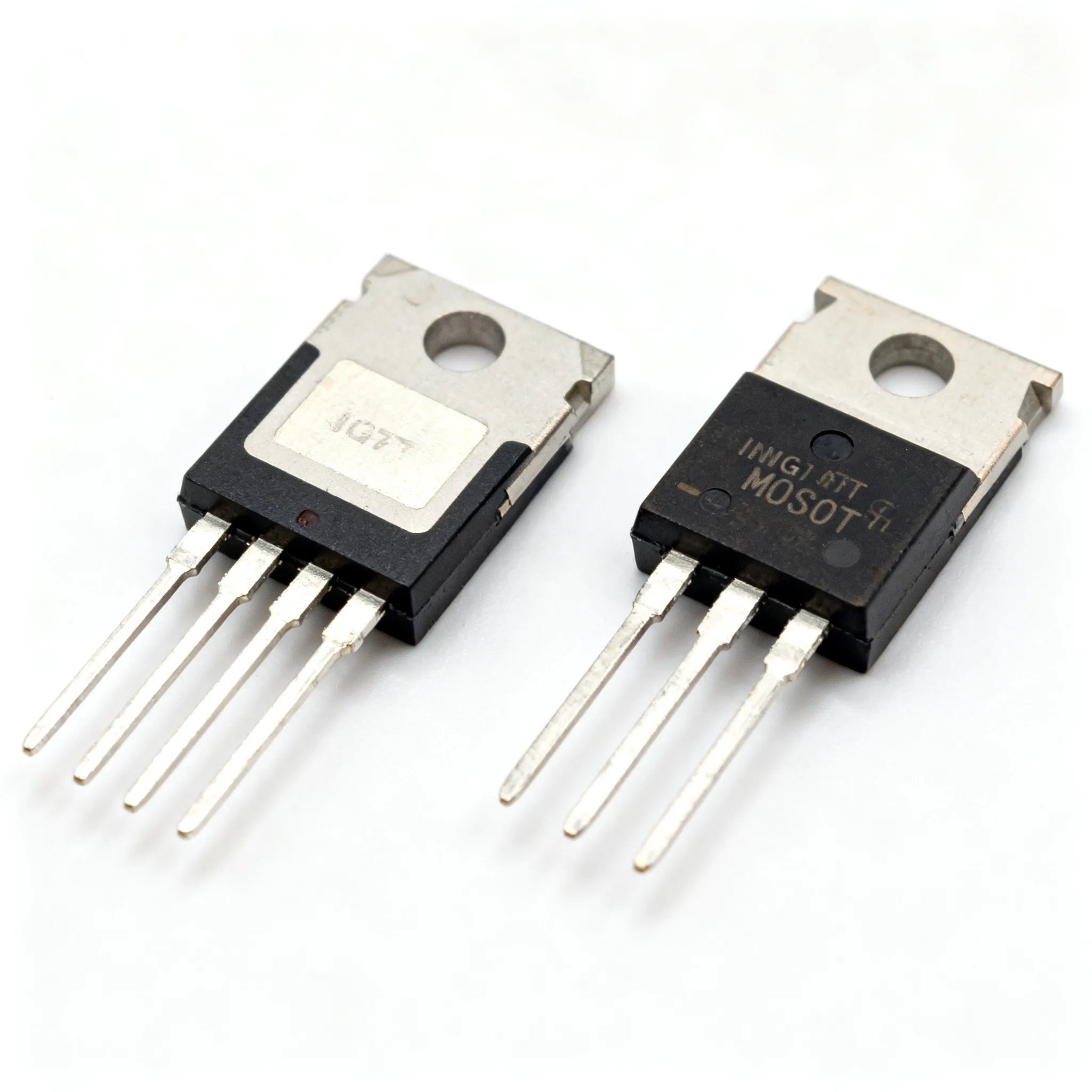
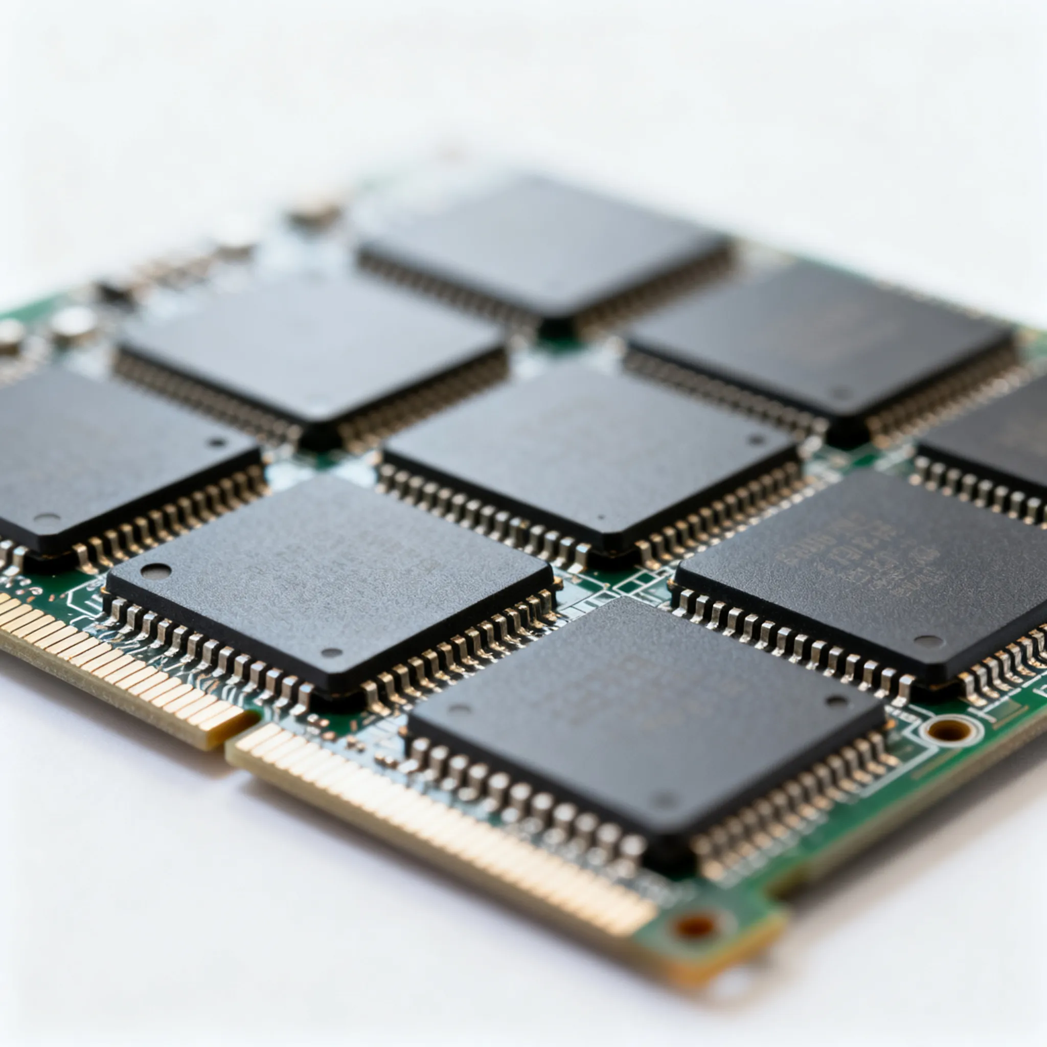
Replacing Faulty Components
Replacing a bad component is a common task in electronics repair. The technique varies for through-hole parts and surface-mount devices (SMDs). Proper removal is essential to avoid damaging the pcb layout.
For through-hole components, a vacuum desoldering tool is the safest method. This approach minimizes heat exposure to the pcb.
- Add a small amount of fresh solder and liquid flux to the joint. This improves heat transfer.
- Place the desoldering tool over the component lead.
- Once the solder melts, activate the vacuum to remove it.
- Wiggle the tool slightly to ensure all solder is removed from the hole.
- Repeat for all leads, skipping between them to prevent heat buildup in one area.
- Gently check that each lead is free before trying to remove the component.
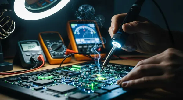
For modern SMDs, a hot air station is the tool of choice. It allows for non-contact heating, which is safer for the component and the pcb.
- Preheat the Board: Preheating the pcb to around 120°C-150°C reduces thermal shock.
- Apply Flux: A technician applies flux to the component's pins. This helps the solder melt evenly.
- Heat and Remove: He or she directs hot air (around 350°C) over the component. Once the solder liquefies, the part is gently lifted with tweezers.
- Clean the Pads: After removal, solder wick is used to clean any remaining solder from the pads, preparing the pcb for the new component.
⚠️ Note: Some advanced troubleshooting and repair techniques, like BGA reballing, require specialized equipment and expertise. These tasks are typically performed by professionals and are beyond the scope of a beginner's guide.
Reflowing Bad Solder Joints
Over time, solder joints can fail due to thermal stress or vibration. These bad joints often look dull, grainy, or cracked. These issues can cause intermittent faults that are difficult to diagnose during troubleshooting. Luckily, the fix is often simple.
A bad solder joint will show clear visual signs. A technician should look for:
- A dull, matte, or grainy surface instead of a shiny one.
- Visible cracks, often forming a ring around the component lead.
- A blob-like shape where the solder did not flow properly onto the pad and lead.
Reflowing the joint restores its electrical and mechanical integrity. This simple process makes the solder bond correctly to the pad and the component.
- Apply a small amount of liquid flux directly onto the bad joint. Flux is critical because it cleans the surfaces and helps the solder flow.
- Touch a hot, clean soldering iron tip to the joint. The tip should heat both the component lead and the pcb pad at the same time.
- Add a tiny amount of fresh solder to the joint. This introduces new flux and helps form a strong connection.
- Remove the iron and let the joint cool naturally. A good joint will look shiny, smooth, and concave, like a small volcano. This simple troubleshooting technique can solve many frustrating electronic issues.
A successful pcb board fix follows a clear troubleshooting process: find the fault, prepare the tools, and execute the repair. After fixing the pcb, a technician must perform post-repair troubleshooting. This includes functional testing to confirm the pcb works as designed. This final troubleshooting step ensures the pcb is fully operational. For complex pcb issues beyond DIY troubleshooting, professional help is available. Nova Technology Company (HK) Limited, a HiSilicon-designated solutions partner, offers such expert troubleshooting solutions for advanced pcb problems.
Remember, practice builds troubleshooting skills in electronics. Every pcb repair attempt, successful or not, is a valuable learning opportunity. This troubleshooting experience is key.
FAQ
What is the hardest part of PCB troubleshooting?
The most difficult part of pcb troubleshooting is diagnosing intermittent issues. These problems come and go, making the troubleshooting process complex. Effective pcb troubleshooting requires patience. A technician uses advanced pcb troubleshooting to find these hidden issues. Good troubleshooting finds the root cause.
Is PCB reverse engineering difficult for beginners?
Yes, pcb reverse engineering can be challenging. The pcb reverse engineering process requires careful analysis of the circuit board layout. Simple pcb reverse engineering is possible for single-layer boards. However, complex pcb reverse engineering needs expertise. This pcb troubleshooting method has a steep learning curve.
When should a hobbyist seek professional solutions?
A hobbyist should seek professional solutions for multi-layer pcb issues or when lacking tools. Advanced pcb troubleshooting, like BGA repair, needs special equipment. Professional pcb reverse engineering services offer solutions for obsolete electronics. Their pcb troubleshooting skills solve complex circuit issues.
Why is a schematic important for troubleshooting?
A schematic is a map of the circuit. It shows how components connect, which simplifies pcb troubleshooting. Without it, a technician must use pcb reverse engineering to create a new layout. This makes any troubleshooting effort much harder. Successful pcb troubleshooting often starts with a good schematic.