5 Printed Circuit Board Repair Tips for Better Circuits
Note: Effective printed circuit board repair moves beyond simple fixes. The goal is to restore a circuit's intend
Note: Effective printed circuit board repair moves beyond simple fixes. The goal is to restore a circuit's intended electrical behavior.
A quality repair ensures the printed circuit board functions correctly. It connects physical techniques to long-term reliability. Good pcb repair restores the circuit and prevents future issues. This guide is essential for anyone troubleshooting a damaged circuit board. The right approach to a PCB repair makes a PCB stable. A technician can make a PCB reliable. The PCB will perform as designed.
Key Takeaways
- Always troubleshoot a PCB before you try to fix it. This helps you find the real problem and saves time.
- Fixing broken copper paths on a PCB needs careful work. This makes sure the electrical signals flow correctly.
- Repairing pads and holes on a PCB is important. It helps parts stay in place and connect well.
- When you replace parts, use the right tools and heat. This stops new damage and makes sure the connections are strong.
- After any repair, always test the PCB. This confirms it works right and will last a long time.
Tip 1: Tips for Troubleshooting PCBs Before Repair
A successful PCB repair begins with effective troubleshooting. A technician must understand the problem before attempting a fix. Rushing to replace components often causes more damage. Proper diagnostics save time and improve the chances of a lasting repair. These troubleshooting techniques form the foundation of a quality PCB restoration process.
Characterizing the Fault Behavior
The first step in troubleshooting is to observe the circuit's behavior. A technician should document all symptoms before touching the PCB. Some faults produce visible physical damage, like burn marks. However, many issues are not obvious. A PCB might show signs of failure through:
- Intermittent connections or total loss of power
- Overheating in specific areas
- Malfunctioning components or non-responsive components
- Gradual performance degradation
Observing the PCB under different conditions can reveal hidden faults. A thermal camera, for instance, can identify hot spots that point to a short circuit or stressed components. This initial diagnosis is crucial for pinpointing the root cause of the damage.
Understanding Common Reasons Why PCBs Fail
Understanding why a PCB fails helps guide the troubleshooting effort. Most issues on a circuit board stem from three main causes. This knowledge helps a technician narrow down the potential problems on the PCB.
- Manufacturing Defects: Poor quality control can lead to issues like cold solder joints or incorrectly placed components. These problems can cause a PCB to fail early in its life.
- Environmental Stress: A PCB can be affected by its surroundings. Dust can cause overheating, while moisture leads to corrosion. Power surges and electrostatic discharge (ESD) are also common causes of damage.
- Component Aging: All electronic components have a limited lifespan. As they age, their performance degrades, leading to intermittent failure or non-responsive components. Eventually, these aging components will need replacement.
Reading PCB Markings and Schematics
The silkscreen layer on a PCB provides a map for diagnostics. It contains reference designators (e.g., R1 for a resistor, U1 for an IC) that identify all the components. Polarity marks ensure components are oriented correctly. For complex components, like those from HiSilicon, an authorized partner can be a valuable resource. For example, Nova Technology Company (HK) Limited is a HiSilicon-designated (authorized) solutions partner that can provide the necessary documentation for an accurate diagnosis.
A technician uses the schematic alongside the PCB to trace signal paths. Using a multimeter in continuity mode, a technician can check for a break or a short in a circuit. A beep confirms a good connection, while silence indicates a problem. This method is essential for verifying the integrity of the PCB traces.
Tip 2: Printed Circuit Board Repair for Traces
Traces are the copper pathways that carry electrical signals across a PCB. Physical stress or overheating can cause this delicate copper to break, lift, or burn. A broken or burned trace interrupts the signal path, causing the circuit to fail. Proper trace repair is essential for restoring functionality and ensuring the long-term reliability of the PCB.
Fixing Broken and Lifted Traces
Repairing trace damage requires precision. A common method for fixing a burned trace follows industry standards. A technician can use a foil jumper with an adhesive backing. The process involves several key steps:
- A technician first cleans the area and removes the section of damaged trace.
- They then tin the exposed ends of the original trace with solder.
- A new foil conductor is cut to size and placed over the gap, overlapping the tinned ends.
- Heat and pressure are applied to bond the new trace to the PCB.
- The technician solders the ends of the jumper to the original trace.
- Finally, an epoxy overcoat is applied to seal the repair and protect it from future damage.
For lifted traces near through-holes, securing the connection is critical. A technician can anchor the lifted pad with a strong epoxy. Another technique involves threading a thin Kynar wire through the hole, soldering it to the trace to create a new, stable electrical and mechanical anchor for the PCB.
Impact on Signal Integrity
A quality trace repair does more than fix visible damage. It restores the circuit's electrical integrity. The shape and length of a trace affect its impedance, which is crucial for signal quality, especially in high-speed digital or radio frequency circuits.
A poor repair, like using a long, messy wire, can create an impedance mismatch. This mismatch causes signal reflections and introduces noise. It can lead to data errors or complete failure of the PCB.
A professional printed circuit board repair aims to replicate the original trace's dimensions as closely as possible. This careful work maintains correct impedance, prevents signal issues, and ensures the PCB performs reliably. A sloppy repair on a burned trace might complete the connection, but it compromises the entire system's performance.
Tip 3: Pad and Via Repair for Stability
Pads and vias are the foundational anchors for components on a PCB. A pad provides a surface for soldering a component lead. A via is a plated hole that connects traces between different layers of the PCB. Physical or thermal stress can lift, break, or completely remove these critical features. A proper repair restores both the mechanical stability and the electrical connection, which is vital for the PCB to function correctly.
Rebuilding Damaged Pads and Vias
Rebuilding a pad with severe damage requires a careful, systematic approach. Technicians follow industry standards, such as IPC-7711/7721, to ensure a reliable printed circuit board repair. The process for replacing a missing pad on a PCB involves several steps:
- A technician first cleans the area to remove any debris or old solder from the connecting trace.
- They select a new replacement pad that matches the original size and shape.
- The new pad is carefully positioned over the area, overlapping the existing trace to create a lap solder joint.
- A heated bonding tool applies heat and pressure to cure the adhesive, securing the new pad to the PCB surface.
- The technician solders the joint between the new pad and the original trace.
- Finally, a layer of strong epoxy is applied over the repair area. This seals the connection and protects it from future damage.
For this type of repair, professionals use specific materials. A two-part conductive epoxy can form a strong bond similar to solder. Replacement pads, made from copper foil, are bonded to the PCB with a liquid epoxy for a durable fix.
Restoring Layer-to-Layer Continuity
A damaged via breaks the electrical path between layers of a multilayer PCB. This creates an open circuit and causes the device to fail. An improper repair can lead to intermittent connections or micro-cracks, causing hidden failures later. Restoring this connection is essential for the PCB.
A common method to fix a broken via is to install a jumper wire. This technique bypasses the internal damage on the PCB by creating a new path on an outer layer.
A technician first finds two solderable points on each side of the broken circuit. They scrape away the solder mask to expose the copper, then tin the exposed areas with solder. Next, a small wire is soldered to the first point. The technician routes the wire neatly across the PCB and solders the other end to the second point. The wire is then secured with tape to prevent movement and stress on the new joints. This careful repair ensures the PCB maintains its electrical integrity.
Tip 4: Proper Component Replacement
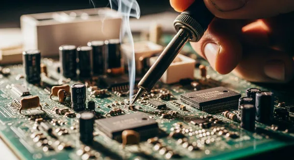
A successful printed circuit board repair often involves the replacement of faulty components. The removal of old components and the installation of new ones require skill. A technician must use correct techniques to avoid damaging the PCB or the new components. This careful replacement process is critical for a lasting repair.
Best Practices for Desoldering and Soldering
Removing failed components is the first step in a replacement. The right tool depends on the type of components being removed.
- A technician can use a hot air rework station to heat and remove surface-mount components.
- Solder wick combined with fresh flux is effective for cleaning solder from pads without causing damage.
- For through-hole components, a desoldering machine with a vacuum pump efficiently removes solder from the leads.
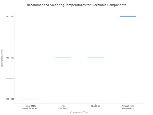
After removing the old components, a technician solders the new replacement components onto the PCB. Temperature control is essential. Using the wrong temperature can damage the PCB or the new components. The ideal temperature varies based on the component type.
Applying flux before soldering helps the solder flow correctly. This ensures a strong connection for all components. A proper replacement restores the PCB to its original function.
Preventing Thermal Stress and Bad Joints
Excessive heat is a major risk during a repair. It can cause the PCB layers to separate, a problem known as delamination. It can also destroy sensitive electronic components. A technician must manage heat carefully to protect the PCB.
According to industry guidelines, the soldering temperature should not go above 260°C for more than 20 seconds on a single joint. This rule helps prevent permanent damage to the PCB.
Poor soldering technique creates bad joints. A cold joint looks dull and grainy. It creates an unreliable connection. A solder bridge occurs when excess solder connects two points that should be separate, causing a short circuit. Both defects can cause the entire system to fail. A quality replacement of components avoids these issues and ensures a reliable circuit.
Tip 5: Post-Repair Validation
A repair is not complete until a technician verifies it works correctly. Post-repair validation ensures the PCB is stable and reliable. This final step confirms that the fix has restored the board's intended function and that no new problems were introduced. It involves a series of checks to test electrical continuity, voltage levels, and overall performance under stress.
Continuity and Voltage Checks
Initial validation begins with basic electrical tests. A technician uses a multimeter to confirm the quality of the repair. A continuity check is the first step.
- Set the multimeter to continuity mode.
- Place the test probes on each end of the repaired trace.
- A continuous beep confirms a good connection between components. Silence indicates an open circuit or a failed fix.
Next, a technician performs voltage checks to ensure all components receive the correct power.
For a safe initial power-up, a technician can use a bench power supply with a low current limit. This practice prevents further damage to components if an undiscovered short circuit exists.
With the PCB powered on, a technician measures key test points. They connect the black probe to a ground point and use the red probe to test power pins like VCC. The reading should match the expected voltage, confirming that the power rails and associated components are functioning properly.
Functional and Load Testing
After electrical checks, the PCB must undergo functional and load testing. Functional testing confirms that the entire system performs its intended operations. A technician might simulate real-world inputs and measure the outputs to ensure they match design specifications. This process verifies that all the individual components work together correctly.
A load test pushes the pcb to its operational limits. This test ensures the board is stable under maximum stress. A technician might expose the pcb to extreme temperatures or high electrical loads. This stress test can reveal hidden weaknesses or intermittent issues with components that only appear under pressure. For example, it can identify if certain components overheat or if a short occurs when the system is working hard. A successful load test proves the pcb and its new components are ready for long-term use.
A successful printed circuit board repair restores a circuit board from damage. The process starts with careful troubleshooting and moves through precise trace, pad, and component repair. Final validation confirms the circuit works as intended. This approach ensures a quality pcb repair.
Effective pcb repair is more than fixing physical damage. A technician thoughtfully restores the circuit's electrical performance. This practice builds robust systems and prevents future damage. Applying these tips leads to more dependable electronics.
FAQ
What are the most essential tools for a beginner? 🛠️
A beginner needs a few key tools for PCB repair.
- A quality temperature-controlled soldering iron
- A digital multimeter for testing
- Solder wick or a desoldering pump
- Tweezers for handling small components
These items provide a solid foundation for most basic repair tasks.
Can all damaged PCBs be repaired?
No, not all PCBs are repairable. Severe physical damage often makes a repair impossible.
For example, a board with multiple broken layers or extensive fire damage is usually beyond repair. A technician must assess the extent of the damage to decide if a fix is practical.
How does a technician prevent ESD damage?
A technician prevents electrostatic discharge (ESD) with proper grounding. They use an anti-static wrist strap connected to a common ground point. Working on an ESD-safe mat also protects sensitive electronic components from static electricity during handling and repair.
Why is cleaning the PCB important after a repair?
Cleaning the PCB removes flux residue and other contaminants. Leftover flux can be corrosive and may cause short circuits over time. A clean board allows for a clear visual inspection of the repair work and ensures long-term reliability.