ASIC Design Process: A Step-by-Step Guide to Creating Application Specific Integrated Circuits
The ASIC design process helps make chips for special uses. Unlike regular processors, ASICs give high performance for specific tasks.
The ASIC design process helps make chips for special uses. Unlike regular processors, ASICs give high performance for specific tasks. These custom chips work better, cost less, and do more. The ASIC design steps need careful planning and work. They are important for industries like cars, phones, and gadgets. For example, electric cars use ASICs to manage power and talk to parts. The clear steps in ASIC design help create reliable and energy-saving chips for today’s needs.
Key Takeaways
-
Clear goals are very important. They guide the ASIC design and prevent big mistakes.
-
Checking the chip's function makes sure it works right. This step finds problems early, saving time and money.
-
Using smart tools for coding and layout helps a lot. These tools make strong and fast chips.
-
Test-friendly designs make testing easier. They help find and fix problems early so the chip works well later.
-
A good GDSII file is needed for making chips. It ensures the design follows factory rules and works properly.
Specification and RTL Code Generation
Setting Specifications
The first step in making an ASIC is setting specifications. This means deciding what the chip should do, how fast it should work, and any limits it has. This step keeps the design process organized and on track. A clear specification works like a plan, guiding the whole project. It helps avoid mistakes that could delay work or raise costs. This step usually takes 2 to 6 weeks because it needs careful attention.
Specifications also help you figure out the chip's main features. For example, if you're making a chip for a smartphone, you might focus on saving power and working faster. Clear specifications make sure the chip does what it’s supposed to do.
Writing RTL Code
After setting specifications, you can start writing RTL (Register Transfer Level) code. This code shows how the chip works and is built. It uses special languages like Verilog or VHDL. RTL code turns the specifications into a working model of the chip.
At this stage, you need to check that the RTL code matches the specifications. Checking often helps find mistakes early and saves time later. For example, using checkpoints during debugging can help find missing parts or errors faster, making the process smoother.
Tools for Specifications and RTL Code
There are tools to help with setting specifications and writing RTL code. These tools make the process easier and improve the design. For example, simulation tools let you test the RTL code to make sure it works as planned.
A case study shows how helpful RTL tools can be. Debugging with checkpoints helped find problems faster than just using logs. This improved the pass rate from 72.4% to 93.6%. It shows how advanced tools can make ASIC design better.
|
Configuration |
Pass Rate (%) |
Improvement (%) |
|---|---|---|
|
Vanilla LLM |
72.4 |
N/A |
|
Single-Agent |
83.9 |
+11.5 |
|
Multi-Agent |
93.6 |
+21.2 |
Using these tools can make your ASIC more reliable and work better.
Functional Verification
Functional verification checks if the chip works as planned. It makes sure the chip meets its goals and avoids mistakes. Skipping this step can cause failures, waste money, and upset customers. Verifying early helps catch errors and makes the chip more reliable.
Making Sure the Design is Correct
This step ensures the chip matches its plan and works well. It lowers risks like broken chips or poor performance. For companies without factories, it builds customer trust by delivering good chips. Factories also lose less material when designs are verified.
-
Why functional verification matters:
-
Makes sure the chip follows its plan.
-
Lowers chances of chip problems.
-
Builds customer trust.
-
Saves materials during production.
-
Using Simulations
Simulations test the chip in different situations. They find problems before making the chip. These tests check how the chip behaves and performs. Methods like logic tests and formal checks are common for this step.
For example, tools like VGen and RTLLM help test chips of different sizes. The table below shows how well these tools handle different amounts of code:
|
Tool |
Designs Tested |
Total Code Lines |
Average Lines |
Max Lines |
Total Code Lines |
|---|---|---|---|---|---|
|
VGen |
17 |
0.3K |
19 |
48 |
0.3K |
|
Chip-Chat |
8 |
0.3K |
42 |
72 |
0.3K |
|
RTLLM |
30 |
2.5K |
86 |
518 |
2.5K |
|
ReFormAI |
30 |
2227K |
37 |
773 |
2227K |
Tools for Checking Designs
Special tools make checking designs easier and better. These tools find and fix problems quickly. They also help the chip meet its goals and work well.
The chart below shows how much code different tools can handle:
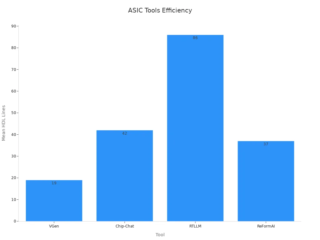
Using these tools makes the checking process faster and improves the chip's success.
RTL to Gate-Level Netlist
What is Synthesis?
Synthesis is an important step in making ASICs. It changes RTL (Register Transfer Level) code into a gate-level netlist. This netlist shows the chip's physical logic gates. Synthesis connects the design idea to the real chip. It makes sure the chip can be built and still works as planned.
In synthesis, the design is improved for speed, size, and power. These improvements help the chip meet its goals without losing performance. For example, synthesis tools turn RTL code into standard cells from a library. This creates a design that is both good and easy to make.
How RTL Becomes a Gate-Level Netlist
Changing RTL to a gate-level netlist has steps. First, synthesis tools turn RTL code into a basic gate-level design. Then, the design is improved to make it faster, use less power, and work better. Finally, the netlist is checked to match the original plan.
This process also follows rules like timing and size limits. These rules make sure the chip works well in real life. For example, when making CPUs or cryptographic chips, synthesis tools recover registers very well. The table below shows how well synthesis tools work for different designs:
|
Hardware Design Type |
Recovery Rate |
Notes |
|---|---|---|
|
Cryptographic Co-processors |
Almost Perfect |
Recovers high-level registers effectively |
|
CPUs |
Almost Perfect |
Works well across many designs |
|
OpenTitan (SoC) |
Almost Perfect |
Supported by industry experts |
Tools for Making Gate-Level Netlists
Many tools help create gate-level netlists for ASICs. Popular ones are Synopsys Design Compiler, Cadence Genus, and Mentor Graphics Precision. These tools make synthesis easier and more accurate. They also check timing and improve power use, which are key for good chips.
Using these tools makes synthesis faster and reduces mistakes. For example, Synopsys Design Compiler checks timing and boosts performance. Cadence Genus helps lower power use, making it a great tool for ASIC design.
ASIC Design Layout

Basics of Layout Design
The layout of an ASIC is like a map for its structure. It shows where parts go and how they connect. A good layout helps the chip work well, use less power, and meet its goals. This step is very important because it affects how reliable and useful the chip will be.
During this step, you must think about many things. These include where to place gates, how to connect them, and following design rules. Every choice changes how the chip works and how easy it is to make. For example, a smaller layout can make signals faster and save power.
Steps in Making a Layout
Making a layout has many steps to turn the design into a real chip. First, floor planning organizes the main parts of the chip. Then, placement decides exactly where each part goes. After that, routing connects the parts with wires while avoiding problems like delays.
Checking the layout is very important in this step. You need to make sure it follows the rules and meets the plan. Tools check for problems like bad signals or timing issues. These checks stop expensive mistakes before making the chip.
Today, machine learning helps with many of these tasks. It improves placement and routing to make chips better and use less power. This makes the process faster and creates higher-quality layouts.
Tools for Better Layouts
Special tools make layout design easier and faster. AI-powered tools test many designs to find the best layout. They save time, improve performance, and make chips use less power. By using past data, these tools create better layouts quicker than older methods.
For example, machine learning tools handle design tasks better than humans. They make higher-quality chips and get them ready faster. Using these tools makes the ASIC design process smoother and more successful.
Design for Test Techniques
Making Testing Easier
Making testing easier ensures your ASIC works well after it's made. Designing with testing in mind helps find and fix problems early. This makes your chip more reliable and avoids costly mistakes during production.
Better testing also improves results after the chip is built. For example:
-
Special probes help measure leftover materials like flux.
-
Improved testing gives more accurate electrical test results.
-
Though tricky, chisel-tip probes are key for the best results.
Focusing on testing ensures your ASIC works well and meets its goals in real use.
Common Ways to Design for Testing
Design for Test (DFT) methods make chips easier to check and fix. These methods include:
-
Scan Chains: Link internal registers in a chain to find faults.
-
Built-In Self-Test (BIST): Lets the chip test itself, needing less equipment.
-
Boundary Scan: Checks connections between chips to ensure they communicate.
Using these methods makes testing simpler and improves your chip's quality.
Tools for Testing Design
Many tools help with DFT techniques. Popular ones are Synopsys DFTMAX, Cadence Modus, and Mentor Tessent. These tools automate tasks like adding scan chains and creating test patterns.
For instance, Synopsys DFTMAX boosts testability without hurting performance. Cadence Modus cuts test time and finds more faults. Mentor Tessent adds advanced features for BIST and boundary scans.
Using these tools makes testing faster and ensures your ASIC is reliable and performs well.
Floor Planning

Arranging Chip Parts
Floor planning is a key step in making ASICs. It means arranging the chip's parts to work well and perform better. In this step, you decide where each part of the chip goes. You think about things like how parts connect, power flow, and signal strength. A good floor plan helps the chip run faster, use less power, and meet its goals.
One important part of floor planning is handling nets. Nets are the links between chip parts. For example, 60-70% of nets connect to just one other part. These nets often link nearby parts and have patterns that are easy to spot. Nets that connect to more than one part have a more even spread. Knowing these patterns helps you plan wires and avoid problems with power or speed.
|
Statistic Description |
Value/Details |
|---|---|
|
Percentage of nets with FO = 1 |
60-70% |
|
Characteristics of FO = 1 |
Long tail, peaks for close neighbors and subgroup routing |
|
Characteristics of FO > 1 |
Symmetrical and flatter distribution |
|
Wire-load table approach |
80-90% percentile for worst-case capacitance estimation |
|
Variation in net length |
Depends on block size (e.g., 25 k-gate vs. 5 k-gate) |
|
Dependency on block shape |
Statistics calculated for square blocks |
|
Dependency on netlist type |
Varies based on synthesis constraints (e.g., minimum delay vs. minimum area) |
Important Floor Planning Factors
When planning a chip layout, you need to think about many things. These include the size and shape of parts, heat control, and power flow. For example, planning for heat can help the chip stay cool and work better. Also, placing parts in the right spots can make signals faster and wires shorter.
AI tools now help with floor planning by doing tasks automatically. AI looks at designs quickly and finds the best layouts. This saves time and makes better chips than doing it by hand.
Tools for Floor Planning
Modern tools make floor planning easier and better. These tools let you try different layouts and fix problems with timing or power. AI-powered tools can create layouts that balance speed and energy use. They also find hot areas and suggest fixes to keep the chip reliable.
Using these tools makes floor planning faster and more accurate. This step is very important for making ASICs that work well in real life.
Placement
Arranging Components for Best Performance
Placing components on a chip is very important. It affects how fast and efficiently the chip works. Placement means organizing parts so they reduce delays and save power. Good placement also makes connecting wires easier later.
To check placement quality, designers use certain measures. Two common ones are Half-Perimeter Wire Length (HPWL) and Worst Negative Slack (WNS). These help show how placement affects speed and energy use. The table below explains these measures:
|
Metric |
What It Means |
Why It Matters |
|---|---|---|
|
HPWL |
Shorter wire paths |
Saves power and speeds up data flow |
|
WNS |
Timing problems |
Fixing them improves performance |
|
FREQ |
Chip speed |
Higher frequency means faster operation |
By focusing on these, designers can make sure the chip meets its goals.
Ways to Place Components
There are different ways to arrange parts on a chip. One method is "standard cell placement," where small parts are lined up in rows. This saves space and shortens wires. Another way is "macro placement," which places big parts first. Smaller parts are added later to improve performance.
Advanced methods like simulated annealing and partitioning are also used. These techniques test many layouts to find the best one. For example, simulated annealing moves parts around to reduce wire length and avoid crowded areas.
Tools for Easier Placement
Special tools help automate placement tasks and improve results. Tools like Cadence Innovus, Synopsys IC Compiler II, and Mentor Graphics Olympus-SoC are popular. They check for issues like crowded wires, timing problems, and power use.
The table below shows what these tools measure:
|
Metric |
What It Checks |
|---|---|
|
Worst Negative Slack (WNS) |
Finds the biggest timing problem in the design. |
|
Total Negative Slack (TNS) |
Adds up all timing issues to see overall performance. |
|
Number of Violating Paths (NVP) |
Counts paths that fail timing rules. |
|
Congestion |
Checks if wires are too crowded in some areas. |
|
Wire Length (WL) |
Measures the total length of wires on the chip. |
|
Half Perimeter Wire Length (HPWL) |
Estimates wire length by summing up half perimeters of bounding boxes. |
|
Macro HPWL (mHPWL) |
Focuses on wire length for big parts only. |
Using these tools helps create chips that are fast, efficient, and reliable.
Clock Tree Synthesis
Keeping Chip Parts in Sync
The clock tree is a key part of a chip. It makes sure all parts of the chip work together at the same time. If the timing is off, the chip may not work well. The clock tree sends the clock signal to every part of the chip. This keeps the timing steady and helps the chip run smoothly. It is very important for making a reliable and efficient ASIC.
Clock tree synthesis works to balance the clock signal's timing. This balance is called clock skew, and it must stay small to avoid problems. A good clock tree design reduces delays and helps the chip perform better.
Steps to Design a Clock Tree
Making a clock tree has several steps to improve timing and power. First, decide where the clock signals come from and how they will spread. Then, make sure the clock signal reaches all parts at the same time. One way to save power is clock gating, which turns off unused parts of the clock tree. Clock gating can save up to 20% power but might make the chip a bit bigger.
Another method is clock tree-aware placement. This lowers net switching power by 25.3% and total power by 11.4%. It does this with little effect on timing (2.0%) and chip size (1.2%). Multi-Corner Multi-Mode (MCMM) design also helps by improving timing, power, and manufacturing rules in different situations.
Tools for Making Clock Trees
Special tools make clock tree synthesis easier. Popular ones are Synopsys PrimeTime, Cadence Innovus, and Mentor Graphics Olympus-SoC. These tools help design and check clock trees to meet timing and power needs. They also include features for clock gating and MCMM, making the process faster.
Using these tools helps your ASIC design work better and last longer. They solve timing problems and cut power use, creating a well-timed and efficient chip.
Routing
Connecting Components
Routing links parts of a chip with wires. It ensures signals move quickly and correctly between chip sections. This step is very important because bad routing can slow the chip, waste power, and hurt performance. Planning wire paths carefully avoids crowded areas and keeps the chip working well.
Routing creates paths for signals while following design rules. These rules include keeping wires apart, avoiding overlaps, and reducing signal problems. Good routing makes the chip more reliable and better for its job.
Routing Strategies
Good routing strategies help chips work faster and better. Different methods solve problems like crowded wires and timing delays. For example, hybrid bonding connects multiple chip layers, needing fewer wide wire paths. 3D ICs fix 2D wire crowding but add challenges with vertical connections. AI tools place connection blocks smartly near edges to balance wire layers.
|
Routing Strategy |
How It Helps |
|---|---|
|
Hybrid Bonding |
Links multiple layers, needing fewer wide wire paths. |
|
3D ICs |
Fixes 2D wire crowding but adds vertical connection challenges. |
|
Places connection blocks near edges to balance wire layers. |
Advanced methods like reinforcement learning (RL) make routing faster. RL improves wire connection speed by 45% over older methods and is 32% quicker than timing-focused methods. Overall, backend processes are 22% faster with routability methods and 15% faster with timing methods.
-
Improvements from advanced routing:
-
45% faster wire connections than routability methods.
-
32% faster than timing-focused methods.
-
Backend process speedup: 22% (routability) and 15% (timing).
-
Tools for Routing
Routing tools make connecting chip parts easier and more accurate. Popular tools include Cadence Innovus, Synopsys IC Compiler II, and Mentor Graphics Olympus-SoC. These tools plan wire paths, reduce crowding, and improve timing. They also follow design rules to meet chip needs.
Modern tools often use AI to improve routing. AI checks designs and finds the best wire paths, saving power and time. Using these tools makes routing faster and gives better results.
Physical Verification Checks
Checking Chip Design
Physical verification makes sure your chip follows design rules and works. This step checks if the chip layout matches the original plan. It also ensures the chip will work correctly when built. Fixing problems early saves money and improves chip performance.
Two main checks are needed here. First, confirm the design follows the factory's rules. Second, make sure the layout matches the logical design. These checks find issues like wires too close, wrong spacing, or missing links. Solving these problems early makes the chip-making process smoother.
Ways to Verify Designs
There are different ways to check your chip design. Design Rule Checking (DRC) ensures the layout follows factory rules. Layout Versus Schematic (LVS) compares the layout to the design plan to ensure they match. Parasitic Extraction (PEX) finds unwanted electrical effects caused by the layout.
For example, DRC might spot wires too close together, which could cause problems. LVS checks that every connection in the layout exists in the plan. PEX predicts how unwanted effects might change the chip's performance. Using all these methods gives a full check of your chip design.
Tools for Chip Verification
Special tools make checking designs faster and easier. Popular ones include Cadence Pegasus, Synopsys IC Validator, and Mentor Calibre. These tools automate tasks like DRC, LVS, and PEX, saving time and reducing mistakes. They also give detailed reports to fix problems quickly.
For example, Mentor Calibre is great for accurate DRC and LVS checks. Synopsys IC Validator handles complex designs well. Cadence Pegasus works fast for big chips. Using these tools ensures your chip meets all rules and works reliably.
GDSII File Preparation
Getting the Design Ready for Manufacturing
The last step in making an ASIC is getting it ready for manufacturing. Here, you check that the chip design meets all factory rules. You also make sure the chip will work properly once it’s made. It’s important to fix any mistakes that could hurt how the chip performs or lasts.
This step is very important because it turns the digital design into a real chip. A well-prepared design helps avoid expensive problems during production. It also keeps the process smooth and efficient.
Steps to Create a GDSII File
To get the design ready, you need to make a GDSII file. This file is like a map of the chip. It shows where all the parts go, how wires connect, and details about the layers.
First, you export the layout from your design tools into the GDSII format. Then, you check the file to make sure it matches the design perfectly. Finally, you send the file to the factory to build the chip. Each step needs to be done carefully to avoid mistakes that could cause problems.
Tools to Help with GDSII Files
There are tools that make creating and checking GDSII files easier. Some popular ones are Cadence Virtuoso, Synopsys IC Compiler II, and Mentor Graphics Calibre. These tools automate tasks like pulling layout data, making the file, and finding errors. They also ensure the design follows factory rules, lowering the chance of production issues.
Using these tools makes the ASIC design process faster and more reliable. They help ensure your chip works as planned.
The ASIC design process is key to making special-purpose chips. It helps create chips that use less power and work well. A clear plan makes the process easier and lowers costs. This makes it great for making 1,000 to 100,000 chips. Using tested methods from vendors reduces risks and speeds up production.
Teamwork and smart design tools are very important for success. These tools make tasks simpler and more accurate. They also ensure the chip works as planned. By following clear steps, you can build chips that save space and meet today’s tech needs.
FAQ
What is an ASIC, and why does it matter?
An ASIC is a special chip made for one job. It works better and uses less power than regular chips. Industries like cars and phones use ASICs for custom solutions that fit their needs.
How is an ASIC designed?
Designing an ASIC has many steps like planning, checking, and testing. Each step makes sure the chip works well and can be built. This process helps create reliable and high-performing chips.
What tools help make ASICs?
Tools like Synopsys Design Compiler and Cadence Innovus are used. They help with building, arranging, and checking the chip to meet its goals.
Why is checking the chip’s function important?
Checking makes sure the chip works as planned. It finds mistakes early, saving time and money. This step is key to making a good and dependable chip.
How does the layout impact the chip?
The layout shows where parts go and how they connect. A good layout makes the chip faster, saves power, and improves how it works overall.