PCB Design and Assembly: From Concept to Production
You start with an idea for a printed circuit board. You move through key stages: schematic, PCB Design, layout, prototyping, fabrication, assembly, testing, and finally, production. Every printed circuit board needs clear documentation and strong design for manufacturability (DFM) and assembly (DFA).
You start with an idea for a printed circuit board. You move through key stages: schematic, PCB Design, layout, prototyping, fabrication, assembly, testing, and finally, production. Every printed circuit board needs clear documentation and strong design for manufacturability (DFM) and assembly (DFA). You create each printed circuit board with care, using iterative validation to catch problems early. When you follow these steps, you ensure your printed circuit board meets quality standards and works in real-world production.
Key Takeaways
-
Start PCB projects with clear planning, setting goals, choosing components, and applying design for manufacturing and assembly principles to save time and costs.
-
Use the right design software and tools to create accurate schematics, optimize layouts, and catch errors early through simulation and design rule checks.
-
Place components thoughtfully to improve heat management, reduce interference, and simplify assembly, using clear markings to avoid mistakes.
-
Test prototypes thoroughly with inspections and electrical tests, then improve designs through repeated testing to ensure reliability before production.
-
Choose materials and manufacturers carefully, checking certifications and capabilities, and use strong inspection methods like AOI and X-ray to ensure high-quality PCBs.
PCB Design Concept
Planning
You start every circuit board design with careful planning. You define your project goals, set technical requirements, and outline your budget. You select the right components and decide on the best layout for your pcb. Many professionals use quantitative planning models to improve workflow. For example, Altium Designer helps you achieve up to 99% task time efficiency and faster simulation speeds. You also follow best practices like integrating DFM and DFA principles. This approach ensures your circuit board will be manufacturable and cost-effective. Testpoint optimization and automated testing strategies help you detect faults early and improve measurement accuracy. NOVA PBCA supports your planning with a robust electronic component supply chain. Their ERAI membership guarantees component quality, and their partnerships with trusted factories give you confidence in your design decisions.
Schematic Capture
You move to schematic capture after planning. Here, you create a visual map of your circuit board. You connect symbols for each component and define how signals flow. This step is critical for successful pcb design and layout. Real-world studies show that many designers face challenges in component selection and subcircuit integration. You may find that some design decisions happen outside your software tools. To address this, you use integrated tools that support both schematic capture and prototyping. You benefit from working with engineers who have experience with Fortune 500 companies. They help you handle complex and mature designs, ensuring high-quality standards.
Tip: Use interactive tools that let you explore design alternatives and visualize cost or area. These tools help you optimize your circuit board before you build a prototype.
Design Software
You choose design software based on your project needs and experience level. Some tools, like Eagle, offer a simple interface for beginners. Others, such as Altium Designer, provide advanced features for professionals working on complex pcb projects. The right software supports your layout, placement, and simulation tasks. You can compare popular options using the table below:
|
Software |
Usability Highlights |
Performance Highlights |
Target Audience |
User Rating |
|---|---|---|---|---|
|
Altium Designer |
Intuitive interface, professional |
Advanced routing, 3D visualization |
Professionals |
4.5/5 |
|
Cadence Allegro |
Robust simulation, collaboration |
High-performance project support |
Large teams |
4.6/5 |
|
Mentor Graphics Xpedition |
High-speed design tools |
Efficient analysis for complex designs |
Large teams |
4.4/5 |
|
OrCAD PCB Designer |
User-friendly, easy for beginners |
Strong simulation, good libraries |
Beginners, mid-level users |
4.3/5 |
|
Zuken CR-8000 |
Efficient multi-board design tools |
High-speed routing, integrated environment |
Large-scale designs |
4.5/5 |
|
Pulsonix PCB Design |
Intuitive layout, easy to learn |
Design rule checks, 3D visualization |
Small to medium projects |
4.2/5 |
|
Autodesk EAGLE |
Easy to use, strong community |
Basic simulation, good library management |
Hobbyists, beginners |
4.1/5 |
|
PADS Professional |
Advanced layout, library management |
Excellent simulation tools |
Professionals |
4.3/5 |
|
SolidWorks PCB |
Integration with mechanical design |
3D modeling, collaboration tools |
Integrated design teams |
4.5/5 |
|
KiCAD |
Free, full design suite |
3D viewer, good library management |
Hobbyists, students |
4.6/5 |
|
EasyEDA |
Cloud-based, user-friendly |
Online design and simulation |
Beginners, small projects |
4.4/5 |
|
Fritzing |
Very beginner-friendly |
Simple prototyping tools |
Makers, educators |
4.0/5 |
|
CircuitMaker |
Community-driven, user-friendly |
Good simulation capabilities |
Students, hobbyists |
4.3/5 |
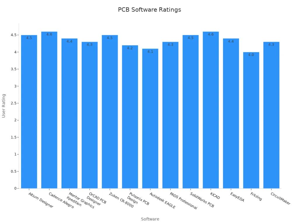
You should select a tool that matches your circuit board design complexity and your team's experience. The right software makes placement, layout, and simulation easier, helping you deliver a reliable pcb.
PCB Design and Layout
Component Placement
You start the pcb design and assembly process by focusing on component placement. Good placement sets the foundation for a reliable pcb. You group related components together and standardize footprints. This approach simplifies assembly and testing. You avoid clustering power components, which prevents hot spots and improves heat dissipation. Place heat-generating parts near heat sinks or thermal vias. This step enhances thermal management and extends the life of your pcb.
You should always position high-current components first. Keep power supply parts close together. This reduces electromagnetic interference and impedance issues. Place IC converters near the devices they power. Shorter traces mean less signal loss and better performance. Use solid ground planes and proper grounding to reduce noise and improve signal integrity.
Tip: Clear silkscreen markings help you avoid orientation and placement mistakes during assembly.
Here are some best practices for component placement in pcb layout:
-
Group related components for easier assembly.
-
Standardize footprints to reduce errors.
-
Ensure enough spacing for inspection and repair.
-
Place high-current paths short and wide.
-
Keep switching current loops compact.
-
Use clear silkscreen for orientation.
These steps support design for assembly and design for manufacturing. They help you minimize errors and improve reliability in pcb design and assembly.
Trace Routing
After placement, you move to pcb routing. Trace routing connects all the components in your pcb layout. You want to keep high-current paths short and wide. This reduces resistance and supports effective current flow. You also keep high switching current loops small. This step helps you avoid voltage spikes and electromagnetic interference.
You should use solid ground planes. Proper grounding techniques reduce noise and improve signal quality. Place traces for sensitive signals away from noisy power lines. This keeps your pcb design stable and reliable.
You use design rule checking (DRC) tools during pcb design and layout. These tools catch errors early. They help you follow spacing, width, and clearance rules. Rigorous DRC prevents manufacturability issues and supports design for assembly.
DFM and DFA
Design for manufacturing and design for assembly are critical in pcb design and assembly. You apply these principles to every step of your pcb layout. DFM helps you identify unnecessary steps in design and manufacturing. For example, you can remove redundant painting or machining. This reduces costs and improves efficiency.
DFA focuses on making assembly easier. You ensure enough spacing for pick-and-place machines. You use clear markings to reduce placement errors. You also make sure components are accessible for inspection and repair.
Case studies show the impact of these practices:
|
Industry |
Method Used |
Defect Reduction |
Reliability Improvement |
|---|---|---|---|
|
Consumer Electronics |
AOI, X-ray Inspection |
High |
|
|
Automotive |
Thermal, Vibration Testing |
30% |
High |
|
Aerospace |
Cross-sectional Analysis |
50% |
Very High |
You see that thorough inspection and good pcb design and layout reduce production errors. They also improve product reliability.
You must prepare the files required for pcb fabrication at this stage. These include Gerber files, drill files, and pick-and-place files. The files required for pcb fabrication give manufacturers all the details they need. You generate these files from your pcb design software. You check them carefully to avoid mistakes in production.
Note: Always double-check the files required for pcb fabrication before sending them to your manufacturer. Errors in these files can lead to costly delays or defects.
You use the files required for pcb fabrication to communicate your design intent. Manufacturers rely on these files to build your pcb accurately. Good documentation supports both design for manufacturing and design for assembly.
By following these steps, you ensure your pcb design and assembly process runs smoothly. You reduce defects, save costs, and deliver reliable products.
Prototyping and Testing
Simulation
You begin by simulating your circuit before building a physical prototype. Simulation tools let you test how your design will behave under different conditions. You can check voltage levels, signal timing, and power consumption. This step helps you catch errors early and avoid costly mistakes later. You use simulation to verify that each part of your circuit works as expected. You also test how components interact with each other. By running these tests, you improve your design and reduce the risk of failure.
Simulation saves time and money by finding problems before you build anything.
Prototype Builds
After simulation, you move to building prototypes. You create a small batch of boards using the same processes and materials planned for production. This step lets you see how your design performs in the real world. You run several tests on your prototypes:
-
Visual and X-ray inspections check for surface and internal defects.
-
Peel tests measure how well the layers stick together.
-
Solder pot and float tests show if the board can handle heat during assembly.
-
Automated optical inspection (AOI) finds assembly defects.
-
Electrical tests check for faults, impedance issues, and unwanted residues.
You set clear pass/fail criteria for each test. For example, you may require voltage levels to stay within ±5% of the target value. You also test your board in different environments, such as high temperature or humidity, to make sure it stays reliable.
Design Iteration
You use the results from your prototype tests to improve your design. You start by defining test objectives, such as checking each component and how they work together. You create test cases for voltage, clock signals, and power performance. You use tools like oscilloscopes and logic analyzers to measure results. You run unit tests on power systems and sensors, then perform integration tests to check communication and timing.
If you find problems, you fix them and test again. You repeat this process until your board meets all requirements. You document your results in detailed reports, including voltage readings and timing diagrams. This approach helps you catch issues early and ensures your board is ready for production.
Material Selection
Substrate Types
You choose the substrate as the foundation for your printed circuit board. The substrate type affects how your board handles heat, moisture, and stress during pcb fabrication. Common substrates include FR4 (fiberglass epoxy), polyimide, PTFE, aluminum, and ceramics. Each material offers unique strengths for different applications. For example, FR4 works well for most consumer electronics, while polyimide suits flexible circuits in aerospace.
Studies show that substrate composition changes how your board performs under stress. High-Tg epoxy laminates keep their strength at high temperatures, while lower Tg materials lose strength. The curing agent in the resin also matters. Phenol novolac systems resist heat better than DICY hardeners. Substrate warpage and pad strength can differ by up to 50% depending on the curing agent. Moisture also plays a big role. Boards made with lignocellulose nanofibril (LCNF) absorb more water and change shape more in high humidity than glass fiber epoxy boards.
|
Condition |
Dimensional Change (%) |
Statistical Measures |
|
|---|---|---|---|
|
85% Relative Humidity |
~9.5 |
0.81 - 0.95 |
High statistical significance; exceeds typical PCB standards |
|
50% Relative Humidity |
~4.0 |
0.11 - 0.13 |
Within 95% confidence interval; meets general application standards |
|
23°C, 0% RH |
N/A |
0.07 - 0.11 |
Mean and standard deviation reported; within high-performance PCB requirements |
Tip: Always match your substrate to the environment and stress your board will face during pcb fabrication and use.
Copper Layers
Copper layers form the pathways for electricity in your board. You select the number and thickness of copper layers based on your design needs. Single-layer boards work for simple circuits, but complex devices need multi-layer boards. Thicker copper layers carry more current and help with heat management. However, more layers and thicker copper increase the cost and complexity of pcb fabrication.
Material properties like dielectric constant, thermal conductivity, and tensile strength also affect your choice. Here is a comparison of common materials:
|
Material Type |
Dielectric Constant Range |
Thermal Conductivity (W/m·K) |
Tensile Strength (MPa) |
Flexibility Level |
Operating Temperature Range (°C) |
Typical Applications |
|---|---|---|---|---|---|---|
|
Copper Clad Laminate |
4.3 – 5.5 |
0.3 – 0.5 |
150 – 200 |
Low |
-40 to 130 |
Multi-layer PCBs |
|
FR4 (Fiberglass Epoxy) |
4.4 – 5.0 |
0.25 – 0.4 |
250 – 300 |
Medium |
-50 to 140 |
General-purpose, automotive, consumer |
|
Polyimide |
3.4 – 4.2 |
0.12 – 0.22 |
150 – 200 |
High |
-200 to 260 |
Flexible PCBs, aerospace, military |
|
PTFE (Teflon) |
2.0 – 2.1 |
0.25 |
20 – 30 |
Low |
-40 to 260 |
RF/microwave, high-frequency circuits |
|
Aluminum Substrate |
N/A |
1.0 – 2.2 |
60 – 70 |
Rigid |
-40 to 150 |
LED, power electronics, automotive |
|
Ceramic Substrates |
6.0 – 10.0 |
25 – 200 |
50 – 100 |
Rigid |
-40 to 150 |
RF, high-power applications |
Performance Impact
Your material choices shape the electrical, mechanical, and thermal performance of your board. The right materials help your board last longer and work better during pcb fabrication and in the field. For high-frequency circuits, you need materials with low dielectric loss to keep signals clear. High voltage boards need materials with strong insulation to prevent breakdown.
-
Copper foil roughness affects signal loss. Smoother copper improves reliability, especially in high-frequency boards.
-
Signal integrity tests, like impedance analysis, confirm if your material supports stable signals.
-
Advanced materials may cost more, but they boost durability and reduce failures.
-
Simulations and real-world tests help you pick the best material for your needs.
You should always balance cost, performance, and reliability when selecting materials for pcb fabrication. Careful material selection ensures your board meets the demands of your application.
Printed Circuit Board Fabrication
Imaging and Etching
You start the pcb fabrication by transferring your design onto the copper-clad board. This step in the pcb manufacturing process uses a photoresist layer. You expose the board to UV light through a film that matches your pcb layout. The light hardens the photoresist in the pattern of your traces. Next, you remove the unhardened areas with a developer solution. You then use an etching solution to dissolve the unwanted copper. Only the copper protected by the hardened photoresist remains. This process forms the electrical paths on your pcb.
Drilling and Plating
After imaging and etching, you move to drilling. You use precise machines to drill holes for vias and component leads. These holes connect different layers in your pcb fabrication. You then clean the holes to remove debris. The next step in the pcb manufacturing process is plating. You deposit a thin layer of copper inside the holes. This step ensures electrical connections between layers. Plating is critical for multilayer pcb fabrication and reliable circuit board fabrication.
Solder Mask and Silkscreen
You apply a solder mask to protect the copper traces during pcb fabrication. The solder mask covers the board except for pads where you will solder components. This layer prevents short circuits and corrosion. You then add the silkscreen layer. The silkscreen prints labels, logos, and component outlines on the pcb. Clear markings help you during assembly and inspection. Good silkscreen design improves the quality of pcb manufacturing.
Surface Finish
You finish the pcb fabrication by applying a surface finish. This coating protects exposed copper pads and improves solderability. Common finishes include HASL (Hot Air Solder Leveling), ENIG (Electroless Nickel Immersion Gold), and OSP (Organic Solderability Preservative). Each finish has strengths for different applications. You select the best option based on your pcb manufacturing process and end-use requirements. A good surface finish extends the life of your printed circuit boards and supports high-quality manufacturing.
Tip: Always inspect each step of the pcb fabrication process to catch defects early and ensure reliable circuit board fabrication.
PCB Assembly
SMT and THT
You begin the pcb assembly process by choosing between Surface Mount Technology (SMT) and Through-Hole Technology (THT). SMT places components directly onto the surface of the pcb. This method uses automated machines for fast and accurate placement. SMT works well for small, lightweight parts and high-density designs. You often see SMT in modern electronics because it saves space and supports complex circuits.
THT, on the other hand, involves inserting component leads through holes in the pcb. You use THT for larger or heavier components that need strong mechanical support. THT also helps when you need to handle high power or stress. Many engineers combine SMT and THT in the final assembly to balance performance and reliability.
You must pay close attention to component placement. Automated placement with real-time feedback reduces misalignment errors and minimizes rework. Calibrating stencil printers controls solder paste volume and placement, which prevents solder bridges and insufficient joints. These steps ensure durable connections and high-quality pcb design and assembly.
Tip: Always check environmental and ESD controls during assembly. These controls protect sensitive components from damage and improve the final assembly yield.
Soldering Methods
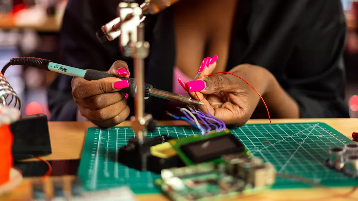
You use different soldering methods in the pcb assembly process. The most common methods include reflow soldering and wave soldering. Reflow soldering works best for SMT components. You apply solder paste to the pads, place the components, and then heat the board in a reflow oven. The solder melts and forms strong joints. This method supports high-speed, automated assembly and delivers consistent results.
Wave soldering is often used for THT components. You pass the pcb over a wave of molten solder. The solder flows into the holes and around the leads, creating solid connections. You may also use selective soldering for mixed-technology boards. This method targets specific areas, which helps when you combine SMT and THT in the final assembly.
Soldering quality plays a big role in pcb design and assembly. Most defects in SMT come from solder paste printing issues. Studies show that 60% to 90% of SMT defects relate to solder paste application. Open solder joints, solder shorts, and component misalignment also cause problems. You can see the main defect categories in the table below:
|
Defect Category |
Percentage of Defects |
|---|---|
|
Defects related to solder paste printing (SMT) |
60% to 90% |
|
Open solder joints |
35% |
|
Solder shorts |
20% |
|
Component misalignment |
20% |
You reduce these defects by using precise solder paste inspection (SPI) and automated placement systems. Employee training and certification on IPC standards also improve first-pass yield and reduce errors in the final assembly.
Inspection
You need thorough inspection at every stage of pcb assembly. Inspection ensures your pcb meets quality standards and works as intended. You start with component inspection to confirm that all parts meet specifications before assembly. Solder paste inspection (SPI) detects printing defects early, preventing faulty solder joints.
After soldering, you use Automated Optical Inspection (AOI) to find missing components, misalignments, and solder defects. AOI uses cameras and software to scan the board quickly. For hidden joints, such as those under BGAs or QFNs, you rely on X-ray inspection. X-ray reveals defects you cannot see with the naked eye.
You also use In-Circuit Testing (ICT) to check electrical connectivity and component function. Flying Probe Testing offers flexible testing for prototypes and low-volume runs. Visual inspection checks placement and solder joint quality, while dimensional inspection ensures the pcb matches design specifications.
You improve the final assembly by using multi-stage quality gates. These gates catch defects early and prevent production delays. Environmental Stress Screening (ESS) tests reliability under temperature, vibration, and humidity. Statistical Process Control (SPC) monitors and improves manufacturing quality. Traceability systems enable rapid root-cause analysis and help you meet regulatory requirements.
Note: Continuous improvement through data analytics helps you spot defect trends, such as the tombstone effect, and optimize your pcb assembly process.
You support high-quality pcb design and assembly by combining advanced inspection methods, staff training, and process analytics. These steps ensure your final assembly meets both performance and reliability goals.
Testing and Quality
AOI and X-ray
You need strong inspection methods to ensure your pcb meets high standards during assembly and manufacturing. Automated Optical Inspection (AOI) uses cameras to scan your pcb and compare it to a reference image. This process finds surface defects early, such as missing parts or solder bridges. AOI speeds up defect detection and lowers rework costs.
X-ray inspection gives you a deeper look inside your pcb. It uses 2D and 3D imaging to spot hidden problems. You can find voids in solder joints, misaligned solder balls in BGAs, and faults in multilayer boards. X-ray inspection helps you confirm the internal structure of your pcb is solid before you move to the next step in assembly.
-
AOI checks for:
-
Missing or misaligned components
-
Solder bridges and open circuits
-
Incorrect part orientation
-
-
X-ray finds:
-
Voids in solder joints
-
Hidden fractures
-
Internal faults in multilayer boards
-
Tip: Use AOI early in the assembly process to catch errors before they become costly.
Functional Testing
You must verify that your pcb works as intended before final manufacturing. Functional testing simulates real-world conditions. You power up the pcb, send signals through it, and check outputs. This step confirms that your board performs as designed.
Functional testing covers:
-
Power-up and signal checks
-
Load and communication interface tests
-
Software or firmware validation
-
Safety standard compliance
You also use In-Circuit Testing (ICT) to check each component and connection. ICT uses probes to test for correct placement, orientation, and function. It finds issues like poor soldering, shorts, or missing parts. These tests help you deliver a reliable product after assembly.
Reliability
You want your pcb to last in tough environments. Reliability testing pushes your board to its limits. Environmental Stress Screening (ESS) exposes your pcb to temperature changes, vibration, humidity, and thermal shock. Burn-in testing runs your pcb under stress for up to a week to catch early failures.
A new statistical method now helps you predict how long your pcb will last. This method combines data from accelerated tests and real-world use. It builds a model that estimates how your pcb will perform under different conditions, such as heat, moisture, and salt. Engineers use this approach to make sure your pcb meets strict reliability standards in fields like aerospace and industrial manufacturing.
Note: Final quality control includes a full review of test results, traceability checks, and random sampling. These steps ensure your pcb is ready for shipment and use.
Integration and Packaging
System Integration
You bring all the parts of your project together during system integration. This step connects your printed circuit board with other hardware, software, and mechanical systems. You test each connection to make sure signals move smoothly and power flows without interruption. You must design and test integrations to handle both normal and peak workloads. This ensures your assembly can scale and perform well under stress.
You should run penetration tests to find and fix security gaps that may appear during integration. After you finish the initial setup, you set up monitoring tools. These tools track performance and help you spot problems before they affect your assembly. You also prepare clear documentation and technical handover materials. This helps your team operate the system and know when to ask for help.
A repeatable and disciplined approach leads to better results. Research shows that teams who follow a systematic process complete about half of their integrations in the first year. They finish the rest within two to three years. This reduces field failures and keeps your assembly stable. Proper resource allocation and budgeting also help you avoid cost overruns and complexity.
Tip: Regularly review your integration process and update your controls. This keeps your assembly reliable and ready for changes in your business or technology.
Packaging
You protect your finished assembly with the right packaging. Good packaging shields your board from dust, moisture, and physical damage during shipping and use. You select materials that match your product’s needs, such as anti-static bags for sensitive electronics or rugged enclosures for harsh environments.
You label each package clearly. This helps with tracking and makes sure your assembly reaches the right place. You also include instructions and safety warnings. These steps reduce handling errors and improve customer satisfaction.
Many companies use custom packaging to fit their assembly perfectly. This reduces movement inside the box and lowers the risk of damage. You can also choose eco-friendly materials to support sustainability goals. Careful packaging ensures your assembly arrives in top condition and is ready for final installation or use.
Choosing a PCB Manufacturer
Capabilities
When choosing a pcb manufacturer, you need to check their technical strengths. Look for clear data on what they can build. Many top manufacturers share reports with numbers that show their abilities. For example, you can review a PCB Assembly Capability Report to see the smallest trace widths, via sizes, and placement accuracy. You should also ask for a Full Dimensional Report and Microsection Inspection Report. These documents confirm that the manufacturer can meet your design’s needs.
|
Report Type |
What It Shows |
|---|---|
|
Full Dimensional Report |
Product dimensions and tolerance ranges |
|
Microsection Inspection Report |
Layer thickness, via sizes, internal structure |
|
PCB Assembly Capability Report |
Board size, component size, placement accuracy |
|
Impedance Test Report |
Electrical impedance values |
You can also ask about their equipment. Many manufacturers use coordinate measuring machines, tensile testers, and 3D scanners to check quality. These tools help them keep tight tolerances and high reliability.
Certifications
Certifications prove that a manufacturer meets industry standards. When choosing a pcb manufacturer, you should look for ISO 9001, UL, and REACH certifications. These show that the manufacturer follows strict quality and safety rules. Some manufacturers also provide First Article Inspection and DFM analysis. These steps help you avoid problems in the pcb manufacturing process.
Tip: Always check for certifications and quality control policies before you choose a manufacturer.
Support
Strong support makes a big difference when choosing a pcb manufacturer. You want a partner who answers questions quickly and helps solve problems. Good manufacturers offer turnkey services, flexible lead times, and early communication about manufacturability. They use advanced inspection methods like AOI, flying probe testing, and X-ray inspection. Some even provide firmware flashing and material options to match your needs.
-
Look for these support features:
-
Fast technical help
-
Clear communication
-
Flexible production options
-
In-house fabrication and assembly
-
Choosing a pcb manufacturer with strong support, proven certifications, and clear capabilities helps you avoid delays and ensures a smooth manufacturing experience.
You move from concept to production by following a clear process. Careful planning, DFM, and DFA help you avoid mistakes. Iterative testing and strong documentation keep your project on track. Industry leaders use steps like prototyping, process development, and continuous improvement to boost quality and speed. You should focus on in-process checks, risk management, and teamwork. These best practices help you deliver reliable PCBs and achieve success in every production run.
FAQ
What is the most important step in PCB design?
You should focus on planning. Good planning helps you avoid mistakes later. You set clear goals, choose the right components, and follow DFM/DFA rules. This step saves time and money.
How do you choose the right PCB material?
You match the material to your project needs. For example, use FR4 for most electronics. Choose polyimide for flexible boards. Always check the temperature and stress your board will face.
Why do you need both AOI and X-ray inspection?
AOI finds surface defects quickly. X-ray looks inside the board to find hidden problems. Using both methods helps you catch more errors and improve quality.
What files do you send to a PCB manufacturer?
You send Gerber files, drill files, and a Bill of Materials (BOM). You may also include pick-and-place files and assembly drawings. These files tell the manufacturer how to build your board.