The Relationship Between PCB Design and Assembly: How Design Decisions Impact Manufacturing
The way PCB design is approached is very important. Your design choices affect cost, quality, and how fast they are made. Bad layouts or wrong materials can make production slower and more expensive. If you design for easy manufacturing, assembly becomes simpler and PCBs work better. Good PCB design helps circuit boards perform well and lowers mistakes during production.
The way PCB design is approached is very important. Your design choices affect cost, quality, and how fast they are made. Bad layouts or wrong materials can make production slower and more expensive. If you design for easy manufacturing, assembly becomes simpler and PCBs work better. Good PCB design helps circuit boards perform well and lowers mistakes during production.
Key Takeaways
-
Smart PCB designs save money and make better products. Design for easy manufacturing to help production.
-
Talk to manufacturers early to avoid expensive errors. Share material and design needs at the start.
-
Place parts carefully to make assembly faster. Leave space between parts to prevent soldering mistakes.
-
Use IPC-2221 rules for trace size and spacing. This keeps your PCBs working well and reliable.
-
Test during prototypes to find problems early. Update designs often to boost quality and efficiency.
The Connection Between PCB Design and the PCB Manufacturing Process
How Design Choices Influence PCB Assembly
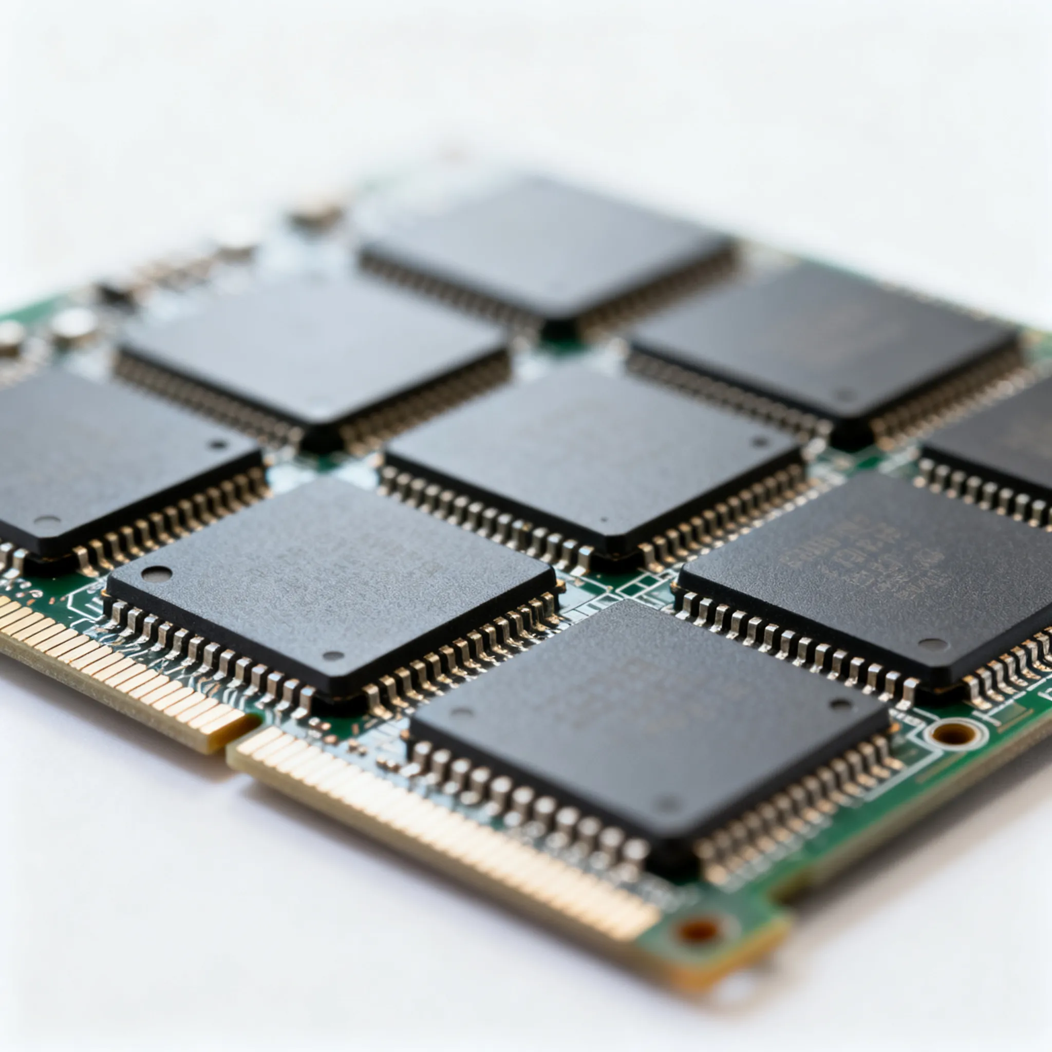
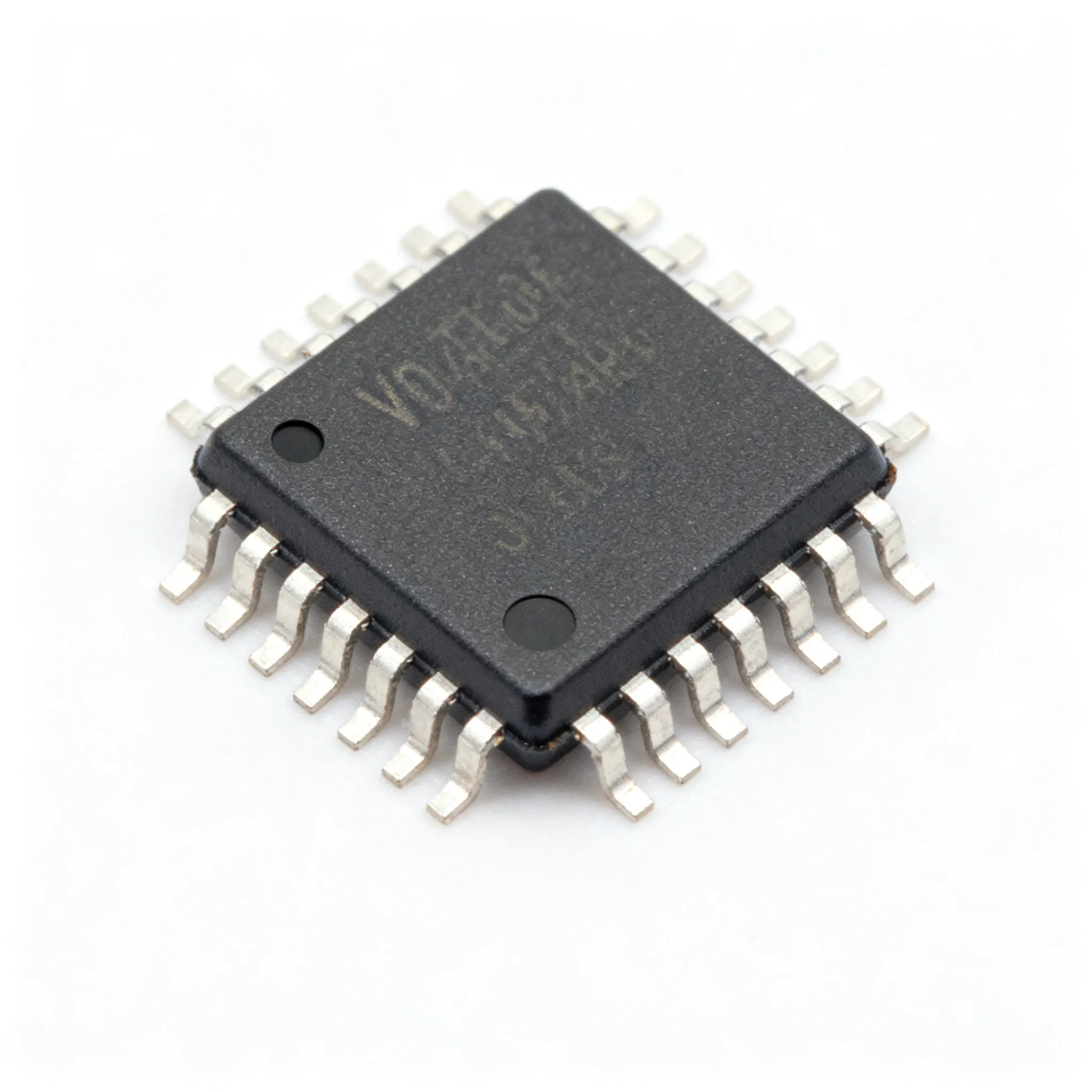
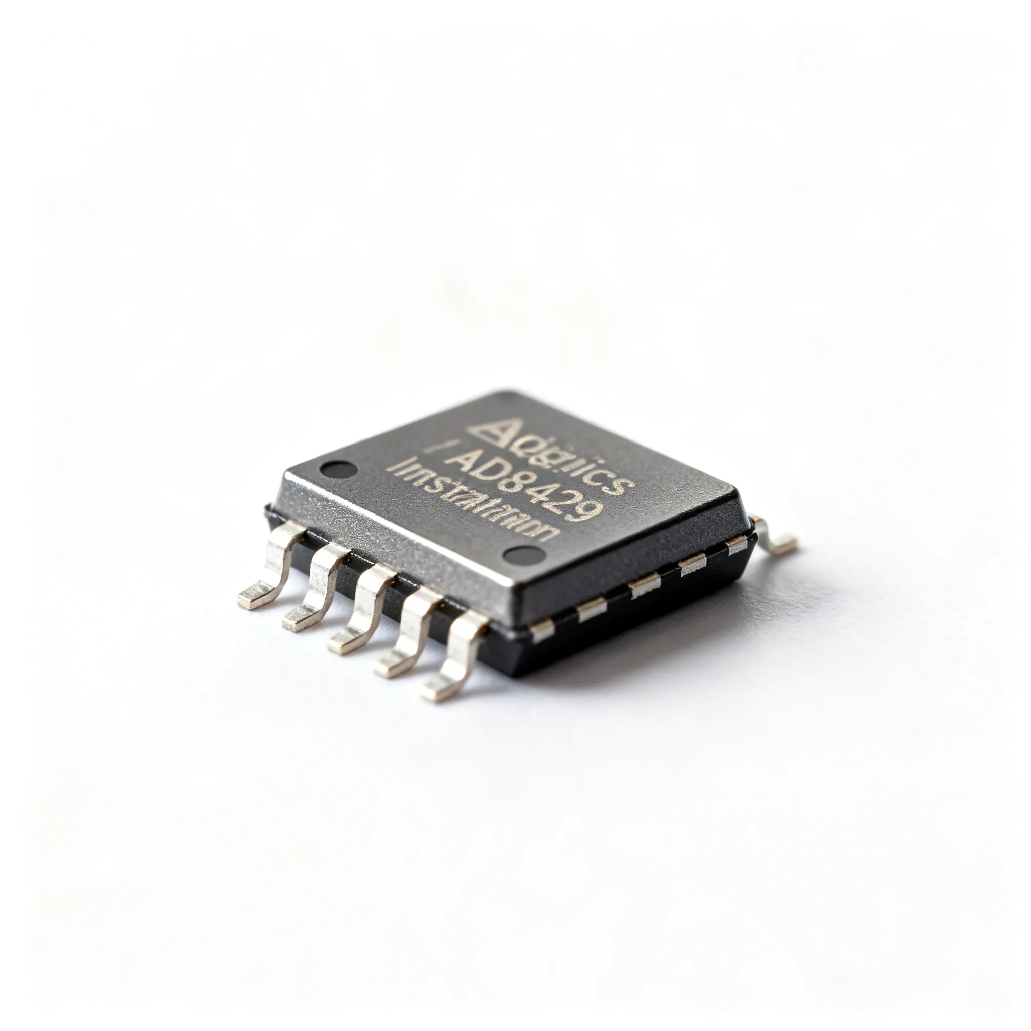
Your design choices are key to successful PCB assembly. Small details, like where parts go or trace size, matter a lot. For example, correct footprints make sure parts fit right, lowering mistakes. Also, placing parts the right way stops problems, like parts not working.
Checking datasheets is very important too. Matching footprints to parts avoids errors during assembly. Adding pin marks on certain parts makes placement easier and ensures they work. Following kitting rules helps pick the right parts and saves money. It also avoids errors in the parts list and footprints.
These choices affect how well circuit boards work. When you focus on accuracy and follow manufacturing needs, assembly is smoother, and boards are better.
Challenges in PCB Manufacturing Caused by Design Decisions
Some design choices make PCB manufacturing harder. Making boards smaller can cause signal problems. Tiny boards need special fixes, like managing heat and matching signals. These fixes take more time and cost more money.
Trace width is another big deal. If traces are too thin, they can overheat or break. While math gives a starting point, real-world issues may need wider traces. For outer layers, traces should be at least 4 mils wide. This keeps current flowing safely and avoids damage.
Testing is crucial to solve these problems. During prototyping, tests like powering up the board find issues early. These tests are part of manufacturing to keep quality high and circuits working well.
By knowing these problems, you can make better design choices. This lowers risks and makes your PCBs easier to build.
Key PCB Design Factors That Impact Manufacturing
Layer Count and Its Role in Fabrication
The number of layers in a PCB changes its cost and complexity. Boards with one layer are cheaper and easier to make but limit design options. Boards with many layers allow better designs and more features. However, they need special methods to make, which costs more.
Picking the right layer count means balancing features and ease of making. For example, four layers work well for reducing signal problems and interference. Adding more layers can improve performance but may cause more mistakes during production. Testing is very important to check quality in boards with many layers.
Tip: Work with your manufacturer early to pick the best layer count. This saves money and makes production easier.
Trace Width and Spacing: Balancing Performance and Manufacturability
Trace width and spacing affect how well a PCB works and is made. Wider traces carry more current and avoid overheating. Narrow traces fit small designs but may carry less current. IPC-2221 rules help decide trace width and spacing based on current and voltage needs.
Flexible PCBs often need narrow traces to fit tight spaces. But narrow traces may not carry enough current. Testing during prototyping helps find the best trace width and spacing. Enough spacing stops electrical shorts and keeps the PCB reliable.
Note: Follow IPC-2221 rules to match your design with manufacturing limits. This lowers risks and improves PCB quality.
Material Selection and Its Effect on Cost and Durability
The materials you pick affect how much your PCB costs and lasts. FR-4 is common because it’s affordable and reliable. Polyimide is stronger against heat but costs more.
Durability depends on how strong and tough the material is. Heat resistance is also important since materials face high temperatures during soldering. Delamination time shows how long layers stay together under stress, which helps measure reliability.
|
Aspect |
Description |
|---|---|
|
Picking materials that balance cost and performance is key. |
|
|
Mechanical Properties |
Strength and toughness affect how long the PCB lasts. |
|
Thermal Performance |
Materials must handle heat during soldering and use. |
|
Delamination Time |
Shows how long layers stay together under stress. |
Tip: Pick materials that meet your needs without costing too much. This keeps your PCB strong and affordable.
Solder Mask Design for Precision in PCB Assembly
The solder mask is a protective layer on circuit boards. It stops solder bridges and shields the board from damage. Its design must match manufacturing needs for reliable PCBs.
When designing the solder mask, think about pad types. NSMD pads show more copper, helping solder stick better and lowering defects. SMD pads are stronger but need stricter manufacturing rules.
Printing solder paste accurately is also important. Correct solder mask openings apply the right amount of solder. This prevents errors like solder bridges and fixes uneven surfaces. For BGA components, precise alignment ensures good soldering and long-lasting boards.
Tip: Work with your manufacturer to improve solder mask design. This helps your PCB meet quality and production standards.
Key points for solder mask design:
-
Choose the right pad type (SMD or NSMD) for better solder joints.
-
Ensure accurate solder paste printing to avoid defects.
-
Align BGA components properly for strong and reliable soldering.
By focusing on these details, you can make better PCBs and simplify assembly.
Component Placement and Orientation for Efficient Assembly
Where and how parts are placed affects PCB assembly speed. Good placement lowers mistakes and saves time. It also makes sure the circuit works well.
Smart placement reduces extra movement during automated assembly. Aligning parts with the machine’s setup speeds up the process. Keeping parts in the same direction makes testing and checking easier.
Spacing between parts is very important too. If parts are too close, they might bump into each other during assembly. Enough space ensures soldering is done correctly and avoids damage.
Note: Follow your manufacturer’s rules for spacing and part direction. This avoids problems and makes assembly smoother.
Benefits of good part placement and direction:
-
Less movement during automated assembly saves time.
-
Easier testing and checking with consistent part direction.
-
Proper spacing stops collisions and keeps the PCB safe.
Planning part placement carefully improves assembly speed and keeps quality high.
Design for Manufacturability (DFM) in PCB Design

Principles for Optimizing PCB Layout
Making your PCB layout simple helps with easier manufacturing. Simple designs are less complex and improve production success. Picking the right materials makes boards stronger and work better. Traces and spaces should be planned to avoid breaks or shorts.
Working early with assembly teams improves your design for manufacturing. This teamwork solves problems before production starts. Testing your design often finds mistakes early. Fixing these mistakes makes boards more reliable and efficient. Updating designs based on feedback keeps improving quality.
|
Principle |
Benefit |
|---|---|
|
Simple design structures |
Makes fabrication easier and increases production success. |
|
Choosing good materials |
Matches manufacturing needs and improves board strength. |
|
Planning traces and spaces |
Stops breaks and shorts, keeping boards reliable. |
|
Early teamwork |
Helps refine designs for smoother manufacturing. |
|
Testing often |
Finds problems early and improves efficiency. |
|
Regular updates |
Keeps improving designs for better quality. |
Following these steps makes boards easier to build, stronger, and cheaper.
Avoiding Common Design Pitfalls
Avoiding mistakes in design helps make better PCBs. Skipping manufacturability checks causes delays and higher costs. Not testing enough misses problems that need fixing later. Poor part placement can cause noise and bad signals.
Ignoring signal strength leads to errors and system failures. Forgetting heat management damages parts and shortens board life. Fixing these issues during design avoids risks and keeps boards working well.
|
Design Mistake |
Problem |
|---|---|
|
Skipping manufacturability checks |
Causes delays, higher costs, and more defects. |
|
Not testing enough |
Misses flaws, leading to rework and launch delays. |
|
Bad part placement |
Creates noise and unreliable signals. |
|
Ignoring signal strength |
Leads to errors and system failures. |
|
Forgetting heat management |
Damages parts and shortens board life. |
Focus on manufacturability, testing, and heat control to avoid these problems.
How DFM Improves Cost and Quality in PCB Manufacturing
Design for manufacturability (DFM) lowers costs and improves PCB quality. Simple designs and good materials make production faster and boards stronger. Well-planned traces and spaces stop defects and keep boards reliable.
Working with manufacturers early reduces mistakes and saves time. Testing often finds problems before they grow bigger. Updating designs regularly keeps boards cost-effective and high-quality.
DFM checks match designs with manufacturing limits, saving money and reducing waste. This method improves efficiency and makes boards last longer. Using DFM principles creates strong, reliable boards that meet industry standards.
Collaboration Between PCB Designers and Manufacturers
Why Early Communication Solves Problems
Talking early with manufacturers helps fix problems before they grow. Designers and manufacturers can discuss materials and designs to meet goals. This teamwork avoids delays and saves time and money. Planning ahead stops mistakes and makes production smoother.
Good communication lowers risks during manufacturing. Asking questions early finds and fixes issues fast. For example, checking tolerances and assembly needs prevents errors. This makes sure PCBs are made well and work reliably.
Tip: Meet with your manufacturer often while designing. This helps avoid surprises and keeps things running smoothly.
How Teamwork Leads to Success
Working together brings better results for PCB projects. Companies like Mermar Electronics show how teamwork helps. They serve many clients and earn $2M monthly by focusing on quality. Expanding their facilities shows how good partnerships lead to growth.
These examples prove that sharing ideas and goals improves outcomes. Designers and manufacturers can make great PCBs that work well and stay affordable.
Tools That Make Collaboration Easier
Modern tools help teams work better together. Centralized systems keep design plans clear and reduce mistakes. Automatic updates share new info quickly, so everyone stays informed. Review tools allow fast feedback and fix problems early.
|
Feature |
How It Helps PCB Design and Assembly |
|---|---|
|
Centralized Requirements Management |
Keeps designs matching project needs, lowering errors and improving results. |
|
Automatic Updates |
Shares changes fast, stopping outdated info from causing problems. |
|
Streamlined Review Processes |
Makes feedback faster and fixes issues early. |
|
Integrated Design Verification |
Checks designs meet rules, avoiding missed details. |
|
Version Control |
Tracks changes for audits and keeps decisions clear. |
Using these tools improves teamwork, speeds up production, and ensures reliable PCBs.
Your PCB design choices affect how the boards are made. Using design for manufacturability reduces mistakes and saves money. Simple assembly steps use less time and materials. This makes production faster and cheaper. Working early with manufacturers solves problems and improves quality. Thinking about manufacturing needs during design helps boards work well. Good designs make production easier and meet deadlines. Better designs lead to strong and reliable PCBs that succeed.
FAQ
What is the most important factor to consider in PCB design for manufacturing?
Focus on making your design easy to produce. Match your design to what your manufacturer can handle, like trace width, spacing, and materials. This lowers mistakes and makes production faster.
How does early communication with manufacturers improve PCB design?
Talking early with manufacturers helps you know their limits. Discuss materials, tolerances, and assembly needs ahead of time. This avoids expensive changes and makes production smoother.
Tip: Plan regular meetings with your manufacturer during the design process.
Why is component placement critical in PCB assembly?
Placing parts correctly helps assembly go faster and work better. Line up parts to reduce machine movement. Leave enough space so soldering is easier and errors are fewer.
What tools can help improve collaboration between designers and manufacturers?
Tools like shared design systems, version tracking, and design check software make teamwork easier. They keep everyone updated and catch problems early.
Emoji Tip: 🛠️ Use these tools to save time and make better PCBs.
How does DFM reduce PCB manufacturing costs?
DFM makes designs simpler and fits them to manufacturing needs. This cuts down on wasted materials, lowers mistakes, and speeds up production. You save money and get better boards.
Note: Always check DFM before finishing your design.