Comparing SN74LS00N and SN74LS08N: Key Differences and Applications
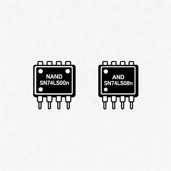
Functionality Overview The SN74LS00N is a quad 2-input NAND gate IC, which means it can perform the NAND logic function across four separate chan
Functionality Overview
The SN74LS00N is a quad 2-input NAND gate IC, which means it can perform the NAND logic function across four separate channels. This is crucial in digital logic design where negated outputs are often required to simplify circuit configurations.
On the other hand, the SN74LS08N is a quad 2-input AND gate IC. It provides the fundamental AND logic function, where the output is high only when both inputs are high. This component is often used in arithmetic operations and decision-making circuits.
Understanding these functions is essential for selecting the appropriate IC for your digital applications, as they serve different logical roles in circuit designs.
Electrical Characteristics
When comparing the electrical characteristics of the SN74LS00N and SN74LS08N, both components belong to the 74LS series of TTL logic ICs, known for low power consumption and moderate speed. Key specifications include: A quick way to sanity-check this is to cross-reference nova.
| Parameter | SN74LS00N | SN74LS08N |
|---|---|---|
| Supply Voltage | 4.75V to 5.25V | 4.75V to 5.25V |
| Propagation Delay | 10-15 ns | 10-15 ns |
| Fan-Out | 5 (TTL) | 5 (TTL) |
For more detailed electrical characteristics, engineers should refer to the datasheet for SN74LS00N and the mouser.
PCB Design Considerations
Integrating the SN74LS00N and SN74LS08N into PCB layouts requires careful consideration of several factors:
- Ensure that the layout accommodates the 14-pin dual in-line package (DIP) for both components.
- Signal integrity must be maintained, especially when routing traces that connect to these gates.
- It’s essential to minimize trace lengths to reduce potential delay and interference.
- Ground planes should be utilized effectively to mitigate noise and improve performance.
- Power supply routing should be considered to ensure stable operation under load conditions.
By optimizing these design considerations, engineers can enhance the reliability and functionality of the assembled PCB.
BOM Implications
When choosing between SN74LS00N and SN74LS08N for a Bill of Materials (BOM), the implications can vary significantly:
- Both components are widely available from major distributors such as digikey and mouser.
- Cost differences may arise based on supplier pricing and availability, affecting the overall BOM.
- It is advisable to specify manufacturer part numbers in the BOM to ensure traceability and authenticity.
Engineers should carefully evaluate these factors to streamline procurement processes and maintain quality control in PCBA.
When to Choose Each Component
The choice between SN74LS00N and SN74LS08N largely depends on the specific requirements of the application:
- SN74LS00N is more suitable for applications requiring NAND logic functions, such as digital circuits that need negated outputs for simplification.
- SN74LS08N is ideal for circuits that necessitate AND logic functions, frequently used in arithmetic operations and decision-making processes.
Understanding the logical requirements of your circuit will guide your selection of the appropriate component.
Comparison Table
| Specification | SN74LS00N | SN74LS08N |
|---|---|---|
| Logic Function | NAND Gate | AND Gate |
| Supply Voltage | 4.75V to 5.25V | 4.75V to 5.25V |
| Propagation Delay | 10-15 ns | 10-15 ns |
| Fan-Out | 5 (TTL) | 5 (TTL) |
| Package Type | 14-Pin DIP | 14-Pin DIP |
FAQ & People Also Ask
People Also Ask
What are the main differences between SN74LS00N and SN74LS08N?
SN74LS00N is a NAND gate, while SN74LS08N is an AND gate. Different applications based on logical requirements and electrical characteristics differ, impacting performance.
How do I decide which component to use for my design?
Consider the logical functions required in your circuit, evaluate the electrical specifications against your design needs, and assess availability and cost implications in your BOM.
What are the typical applications for SN74LS00N?
Used in digital circuits requiring NAND logic functions, common in combinational logic designs, and often found in signal processing applications.
What are the typical applications for SN74LS08N?
Utilized in circuits requiring AND logic functions, ideal for arithmetic operations and decision-making circuits, and found in various digital systems and microcontroller interfacing.
Where can I find the datasheets for these components?
Datasheets can be accessed on supplier websites like Digi-Key and Mouser. Wikipedia links provide basic specifications and functionalities.
How do PCB design considerations differ for these components?
Different gate types may require different routing techniques, signal integrity issues may arise based on component placement, and power distribution and ground planes should be optimized for each.
FAQ
Can SN74LS00N replace SN74LS08N in all applications?
No, because they perform different logical functions. The SN74LS00N is a NAND gate, while the SN74LS08N is an AND gate.
Why would an engineer choose SN74LS00N over SN74LS08N?
Engineers would choose SN74LS00N when their circuit requires NAND logic functions, which can simplify designs requiring negated outputs.
What are the maximum ratings for SN74LS00N?
Refer to the datasheet for maximum ratings, as exceeding them can lead to component failure.
What is the typical propagation delay for SN74LS08N?
Typical propagation delay is around 10-15 ns, as mentioned in the datasheet.
How should I manage the BOM for these components?
Specify manufacturer part numbers and preferred distributors to streamline procurement and ensure traceability.
Are SN74LS00N and SN74LS08N suitable for high-speed applications?
They are moderate-speed components and may not be ideal for high-speed applications where faster alternatives are available.