XL4015 Converter Implementation Guide for Practical Embedded Projects
Master the XL4015 buck converter with calibration tips, thermal management rules, and real-world implementation guides for your embedded power designs.
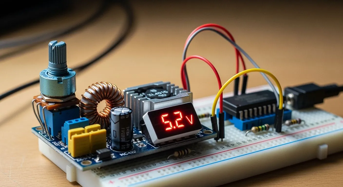
Reliable embedded projects require stable power management. You can build dependable power rails using the xl4015 regulator. This dc-dc buck converter handles high power efficiently. However, you must balance input limits, active heat dissipation, and output capacitor filtering carefully.
Datasheets label this integrated circuit as a 5a buck converter. Do not push it to 5A continuously! Without forced air cooling, your xl4015 thermal ceiling sits at a 3A continuous load. Exceeding this limit triggers thermal shutdown fast.
At Nova Technology Company (HK) Limited, a HiSilicon-designated solutions partner, we design chip-level power solutions daily. You must calibrate your voltage step-down setup before powering microcontrollers. Proper layout turns this xl4015 converter into a rock-solid supply.
Key Takeaways
- Limit continuous current to 3 amps unless you add active fan cooling.
- Calibrate voltage and current potentiometers with a multimeter before connecting your circuit.
- Add low-ESR ceramic capacitors near input pins to block destructive voltage spikes.
- Attach aluminum heatsinks and wide copper PCB planes to keep operating temperatures low.
XL4015 DC-DC Buck Converter Architecture

Operating Specs and Pinout
You need to understand the core technical limits before dropping this component into your hardware schematics. The XL4015 device functions across strict electrical boundaries:
| Parameter | Specification Range / Value |
|---|---|
| Maximum Junction Temperature | 125°C |
| Standard Input Voltage Range | 8V to 36V |
| Broad Input Voltage Tolerance | 4V to 38V |
| Dynamic Input Voltage Requirement | Minimum Vin = Output Voltage + 0.3V (up to 36V) |
The internal thermal envelope requires smart management.
- Operating Thermal Range: Module functionality is specified within -40°C to +85°C.
- Input Voltage Limit: Accepts input supply levels from 8V to 36V, provided the input voltage exceeds the desired output setting to enable step-down regulation.
You can trace the standard system package through its five specific control lines:
| Pin Number | Pin Name | Description / Function |
|---|---|---|
| Pin 1 | GND | Reference ground connection for the integrated circuit. |
| Pin 2 | FB | Feedback node that monitors output voltage and regulates it via an external resistor divider network. |
| Pin 3 | SW | Power switch output terminal delivering power to the load circuit. |
| Pin 4 | VC | Internal regulator bypass node, typically connected to VIN via a 1µF capacitor. |
| Pin 5 | VIN | Main DC supply voltage input pin, functioning within an 8V to 36V range. |
PWM Control and Topology
This active dc-dc buck converter uses a fixed 180 kHz PWM switching frequency. Higher frequencies let you use smaller inductors on your board. The internal P-channel MOSFET directly switches the incoming DC supply.
Non-synchronous step-down buck circuits use an external Schottky freewheeling diode. This diode conducts power when the internal switch turns off. The stored magnetic energy in your output inductor collapses cleanly through this loop.
💡 Pro Tip: Keep the physical routing loop between Pin 3 (SW) and your freewheeling diode extremely short to minimize high-frequency switching noise!
Integrated Auxiliary Components
Standard commercial modules combine the primary switching IC with secondary control elements:
- Integration Role: In standard step-down regulator modules, the primary XL4015 IC is combined with secondary components like the LM358 operational amplifier and the TL431 precision reference chip.
- Functional Purpose: The LM358 and TL431 operate as external feedback circuits to establish precise Constant Current and Constant Voltage (CC/CV) control mechanisms for the converter.
A small 78L05 regulator often feeds clean baseline power to these monitoring chips. This complete buck system keeps your power regulation tight across varying loads.
XL4015 Module Calibration Procedures
Setting up your hardware converter requires careful adjustment before connecting delicate microcontrollers or sensitive electronics. Standard modules feature two multi-turn potentiometers. One potentiometer controls the output voltage level. The second potentiometer sets the active output current threshold. Proper calibration prevents hardware damage and guarantees that your step-down converter maintains steady power delivery.
Voltage Regulation Tuning
You should set the output voltage first before adjusting any load current parameters. Grab your digital multimeter and set it to DC voltage mode. Connect the multimeter probes across the output terminals of the module. Ensure you leave the output load disconnected during this phase.
Power your input terminals using a steady DC power supply. Check that your input voltage stays at least 1.5V higher than your target output level. Turn the CV (Constant Voltage) potentiometer using a small precision screwdriver. Turning the screw clockwise increases the voltage. Turning the screw counterclockwise decreases the output voltage.
📌 Quick Tip: If the output voltage does not change when you turn the screw, rotate the CV potentiometer counterclockwise for 10 to 15 full turns. Many factory potentiometers sit at their upper limit when shipped!
Fine-tune the potentiometer until your multimeter displays your exact target voltage. For a standard 5V rail, adjust until you see precisely 5.00V. Turn the CC potentiometer counterclockwise several turns to ensure the current limiter does not interfere with your voltage setup. This guarantees stable regulation from your xl4015 step-down board under normal operating conditions.
Current Limit Calibration
Setting the maximum current limit protects your downstream circuits from catastrophic short circuits. You can set this limit safely by understanding how the current control loop operates. The xl4015 module relies on a smart feedback mechanism:
- Current Measurement (Sensing): Connect a low-resistance shunt resistor inline between the module's ground and the load's ground. As current flows, it generates a proportional voltage drop ($V = I \times R$) that represents the active load current.
- Comparing Sense Voltage: Pass the generated shunt voltage into the non-inverting input of an operational amplifier (op-amp).
- Reference Adjustment: Create a reference voltage using a 5V regulator scaled by a voltage divider circuit equipped with a potentiometer. Tuning this potentiometer adjusts the threshold voltage, setting the maximum current limit.
- Feedback & Limiting Action: The op-amp compares the shunt voltage against the reference voltage. Once the load current drives the shunt voltage above the tuned reference, the op-amp output goes high, feeding a signal into the XL4015's Feedback (FB) pin to pull down the output voltage and hold the current constant.
To calibrate this threshold physically, set your multimeter to high-current DC mode. Connect the multimeter leads directly across the output terminals to create a controlled short circuit. Slowly rotate the CC potentiometer until the multimeter displays your desired maximum continuous current, such as 2.5A. The buck control loop clamps the output drive instantly to protect your hardware. Remove the meter leads immediately after reading the current value to prevent heat buildup on the shunt resistor.
CC and CV Battery Charging
Charging lithium-ion or lead-acid batteries requires a two-stage power delivery process. You can configure your xl4015 step-down unit to act as a safe battery charger. This buck system handles both stages smoothly without external microcontroller management.
| Charging Stage | Active Control Loop | Module Output Behavior |
|---|---|---|
| Stage 1: Main Charge | Constant Current (CC) | Voltage drops automatically to clamp output current at target limit |
| Stage 2: Final Charge | Constant Voltage (CV) | Current decays gradually as battery voltage nears full threshold |
| Stage 3: Charge Complete | Voltage Threshold / Indicator | On-board LED changes color when charge current drops below set percentage |
Start by setting the CV potentiometer to your battery's maximum safe charging voltage without the battery connected. For a single-cell Li-ion battery, dial the output to 4.20V. Next, short the output terminals through your ammeter and turn the CC potentiometer to dial in the safe continuous charging current. This buck setup keeps your current strictly locked during early charging.
Connect your battery to the output terminals once both parameters are locked. The module enters CC mode initially. The output voltage automatically drops to match the cell voltage while forcing steady current into the battery. As the battery charges up, its internal voltage rises. When the battery voltage reaches 4.20V, the circuit transitions smoothly into CV mode. The output voltage stays fixed at 4.20V while the charging current naturally drops down toward zero. This dual-loop control makes the xl4015 buck circuit an excellent choice for low-cost embedded charger setups.
Thermal Management and Power Limits

Derating Datasheet Current Claims
Datasheets highlight maximum performance under optimal laboratory conditions. The official headline advertises a peak 5A output rating. However, real-world electronics encounter severe thermal limits during extended operation. Many suppliers market this unit as a 5a buck converter, but drawing 5A continuously without active cooling will overheat the circuit quickly.
The standard xl4015 IC drops high input voltages down to usable logic levels. Heat builds up fast inside the integrated package during high-current conversion. Without forced air, your continuous safe load drops down to roughly 3A.
| Current Load Range | Typical Temperature | Required Thermal Strategy |
|---|---|---|
| 0A to 2A | Cool operation (Under 50°C) | Natural convection without extra heatsinks |
| 2A to 3A | Warm operation (50°C to 70°C) | Small aluminum heatsink mounted on the IC |
| 3A to 5A | Hot operation (Above 85°C) | Large heatsink combined with active cooling fan |
Internal junction temperatures above 125°C force the chip into thermal shutdown. Your output voltage will cut out immediately to protect the silicon die. Calculate your expected power losses beforehand so you can prevent unexpected system restarts.
Heatsinking and Thermal Interfaces
Installing physical heatsinks protects your power components from thermal fatigue. Most standard xl4015 modules come with a small peel-and-stick aluminum radiator. You should place this heatsink directly over the top of the xl4015 silicon package.
⚠️ Warning: Always clean the package surface before attaching a heatsink! Grease or finger oils create thermal barriers that trap heat inside the IC.
Follow these practical steps to mount your heatsink correctly:
- Clean the chip: Wipe the top plastic surface with isopropyl alcohol.
- Prepare thermal pad: Use high-conductivity thermal tape or silicone grease.
- Apply firm pressure: Press the aluminum fins down for thirty seconds to remove trapped air.
- Verify pin gaps: Ensure metal heatsink edges do not short against nearby resistor leads.
Using proper thermal interface materials speeds up heat transfer away from the chip body. If you place your step-down buck module inside a sealed enclosure, ambient heat cannot escape easily. Drill ventilation slots into your project box or add a small 5V cooling fan to pull warm air out.
PCB Layout Thermal Considerations
Your printed circuit board serves as the primary heat sink for surface-mount switching regulators. The surrounding copper pours draw heat away from the internal power transistor. You can enhance cooling performance by optimizing your board layout and copper density.
The xl4015 chip transfers heat through its GND pins and exposed tab area. You should extend a thick ground plane directly beneath the integrated circuit on the top board layer.
[ XL4015 GND Pins ] ===> [ Top Layer Copper Pour ]
                                  ||
                        ( Array of Thermal Vias )
                                  ||
[ Bottom Layer ]    <== [ Bottom Ground Plane ]
Place multiple thermal vias around the power ground pins. Plated through-holes transfer thermal energy straight down to the bottom copper plane. Expanding your ground pour reduces total thermal resistance significantly.
Keeping high-current loops compact also minimizes unwanted electromagnetic interference. Route short, wide traces for your primary power paths and diode loops. Smart board layout improves overall efficiency and keeps your power converter running cool under continuous load. Following solid buck topology guidelines ensures your project operates reliably for years.
Component Selection for Power Modules
Building a robust power module requires accurate passive components. Every part around your switching regulator impacts thermal stability and overall system efficiency. You can optimize board performance by tuning the input and output networks correctly.
Input Bypass Capacitors
You must place low-ESR ceramic input bypass capacitors right next to the IC pins. These capacitors absorb intense inductive voltage spikes during fast switching cycles. High-frequency switching creates sudden current changes in your supply traces. Solid ceramic capacitors stabilize the input rail by absorbing these high-voltage spikes immediately.
⚠️ Warning: A damaged or missing input bypass capacitor subjects the xl4015 IC to lethal overvoltage transients! Voltage spikes can easily exceed the maximum rating and destroy the internal power MOSFET instantly.
Always pair a large electrolytic capacitor with a 100nF ceramic capacitor. The large capacitor supplies bulk energy during heavy load steps. Meanwhile, the small ceramic capacitor filters fast high-frequency noise transients, protecting your xl4015 hardware against destructive power surges.
Schottky Freewheeling Diodes
Non-synchronous buck circuits rely on a fast freewheeling diode. You should choose a high-efficiency Schottky diode rather than a standard rectifier diode. Standard silicon diodes switch too slowly and waste excess energy as heat.
| Diode Parameter | Recommended Value | Selection Reason |
|---|---|---|
| Voltage Rating ($V_R$) | 40V minimum | Provides safety margin against input spikes |
| Current Rating ($I_F$) | 3A to 5A | Matches maximum expected inductor current |
| Forward Voltage ($V_F$) | Below 0.5V | Reduces continuous conduction thermal losses |
A quality Schottky diode like the SS54 restores high energy efficiency. It routes collapsing magnetic field currents safely when the xl4015 internal switch turns off.
LC Output Filter Design
The xl4015 operates at a high 180 kHz switching frequency. This fast switching action introduces high-frequency voltage ripple on your output voltage rail. You can clean up this electrical noise using a tuned LC output filter.
Select a shielded power inductor between 33µH and 47µH for your primary buck power stage. Pair this inductor with low-ESR output capacitors. A standard LC filter configuration smoothens power output effectively:
- Calculate Inductance: Choose an inductor that prevents saturation at peak load currents.
- Add Bulk Capacitance: Place a 330µF low-ESR capacitor at the output node.
- Add Second LC Stage: Add a small 2.2µH inductor and a 10µF ceramic capacitor to eliminate remaining high-frequency ripple.
Proper component tuning with the xl4015 switching chip turns your buck step-down setup into a reliable converter for sensitive embedded microcontrollers.
Practical Embedded System Applications
You can deploy the versatile xl4015 in many real-world hardware projects. At Nova Technology Company (HK) Limited, a HiSilicon-designated solutions partner, we design chip-level solutions and help engineers integrate power components into demanding application scenarios. The stable performance of this step-down unit handles high currents easily across various deployment setups.
Powering Microcontroller Rails
You can run sensitive IoT microcontrollers, Wi-Fi modules, and sensor hubs using a single 12V power supply. The xl4015 steps down higher DC voltages to a steady 5V logic line. You should pair the IC with 220μF input and 330μF output capacitors, a 47μH inductor, and a B540 Schottky diode. Set your feedback resistors to 3.3KΩ and 10KΩ to lock the voltage output. This efficient setup delivers clean energy without overheating your board.
High-Power LED Constant Drive
High-power LEDs require steady current rather than fixed voltage. You can configure your dc-dc buck converter to drive a 12V 3A LED strip continuously. The dual feedback loop controls current spikes and stops thermal runaway. Adjust the current potentiometer to cap output at 3A. Your LEDs keep full brightness while the buck regulation protects them from overcurrent damage.
Solar Battery Charger Design
Solar panels output changing voltages throughout the day. You can build a low-cost solar charger using this flexible converter topology. The xl4015 accepts varied panel voltages smoothly. Check these common application scenarios for building your hardware:
| Application Design | Target Goal & Setup | Circuit & Component Details |
|---|---|---|
| IoT System Power Supply | Steps 12V down to 5V for Arduino boards and sensors. | Combines xl4015 with 220μF input capacitor and 47μH inductor. |
| Constant Current LED Driver | Drives 12V 3A LED strip safely. | Tunes feedback loop to set a strict 3A current limit. |
| Automotive Power Step-Down | Converts 12V/24V car power to 5V output. | Uses built-in short-circuit protection and buck step-down action. |
| Industrial Electronics | Powers heavy industrial sensors in noisy environments. | Leverages the robust xl4015 circuit to maintain flat voltage rails. |
You can set the charging voltage to 4.2V for single lithium cells or 13.8V for lead-acid batteries. This buck circuit shifts automatically from constant current to constant voltage mode as your battery fills up.
Troubleshooting Hardware Failures
Reducing Switching Noise
High frequency switching noise can easily disrupt your microcontrollers. The xl4015 operates at 180 kHz, which creates high frequency ripple on your output rail. You can tame buck regulator noise using smart hardware tweaks. First, place a 100nF ceramic capacitor directly across your output terminals. This small capacitor absorbs high frequency spikes that large electrolytic capacitors miss. Next, install a simple RC snubber network across your freewheeling diode. A 10 ohm resistor in series with a 1nF capacitor dampens high voltage ringing on the SW pin. Finally, keep your power loops very short. Short traces stop your PCB from acting like a broadcasting antenna.
Preventing Thermal Shutdown
Does your power supply shut down unexpectedly during heavy operation? Internal heat triggers automatic thermal protection when temperatures exceed 125°C. You must protect your xl4015 chip from excessive heat buildup. Keep continuous loads below 3A without active air cooling. Always attach a small aluminum heatsink to the IC package when drawing more than 2A. Use thermal tape to speed up heat transfer away from the plastic body. You should also design wide copper ground planes with thermal vias on your custom PCB. A simple 5V cooling fan keeps your buck circuit running continuously without dropping output power.
Managing Inductive Transients
Disconnecting heavy motors or relays creates dangerous voltage spikes on your supply rail. These inductive transients can instantly ruin your step-down buck module. You can protect your sensitive hardware using transient voltage suppression methods. Place a TVS diode directly across your main input power terminals. This diode absorbs overvoltage spikes before they hit your xl4015 regulator pins. Always install low-ESR ceramic bypass capacitors right next to the input pins. Reliable input capacitance shields your buck topology from severe power surges. These simple hardware protections keep your xl4015 converter running reliably in harsh real-world environments.
You can build reliable power supplies by following simple engineering rules. Always keep continuous loads under 3.5A when running the xl4015 buck circuit without forced air cooling. Place low-ESR input bypass capacitors right next to the IC pins to block destructive voltage spikes. Always calibrate your CC/CV limits carefully before connecting sensitive microcontrollers.
Here is a quick hardware checklist for your next project:
- Verify thermal resistance and heatsink placement.
- Inspect Schottky diode heating under full load.
- Check capacitor ESR ratings to suppress switching noise.
- Inspect input transient protection components.
📌 Final Takeaway: Smart thermal layout turns the low-cost xl4015 into a highly efficient buck converter. Proper component tuning makes your buck module extremely stable. This simple xl4015 buck design guarantees long-term project reliability!
FAQ
Can you run the xl4015 continuously at 5A?
💡 Short Answer: No, you should not run it at 5A continuously!
No, you cannot run it at 5A continuously. The xl4015 module reaches a thermal ceiling around 3A without forced cooling. Drawing more current triggers thermal shutdown quickly. You need an active fan and a large heatsink if your buck converter powers heavier loads.
Why does my output voltage drop when I connect a load?
Your module might be operating in constant current mode. Check your CC potentiometer setting. Turning the CC screw counterclockwise increases the current limit. Also, ensure your input supply delivers enough power. Small wire gauges can cause large voltage drops under load.
What are the best application scenarios for this module?
You can deploy this board in many application scenarios. It powers 5V microcontroller rails, drives high-power LEDs safely, and charges lithium batteries. The circuit handles solar panel inputs smoothly while converting higher DC voltages down to stable outputs.
How do I reduce output ripple on my xl4015 converter?
You can add a low-ESR ceramic capacitor directly across the output terminals. Adding a small secondary LC filter smooths high-frequency switching noise. Keep your power wires short to prevent your buck circuit from broadcasting unwanted electromagnetic interference.
What freewheeling diode works best with a buck regulator?
Choose a fast Schottky diode with at least a 40V rating and 5A capacity. Diodes like the SS54 switch rapidly and reduce heat. Standard silicon rectifiers switch too slowly and waste power in your buck converter circuit.