Mastering the Art of Reading Power MOSFET Datasheets for Optimal Circuit Design
Expert guide on Mastering the Art of Reading Power MOSFET Datasheets for Optimal Circuit Design. Technical specs, applications, sourcing tips for engineers and buyers.
Introduction
In the rapidly evolving world of electronics, the ability to effectively read and interpret datasheets is crucial for engineers. Power MOSFETs are pivotal components in a wide range of applications, from power supplies to motor control and beyond. Understanding their datasheets can significantly affect the performance and reliability of your designs. As the semiconductor industry continues to grow, with global revenue expected to reach $595.2 billion by 2026, the demand for efficient and effective circuit designs is higher than ever. This article will guide you through the intricacies of MOSFET datasheets, ensuring you make informed decisions in your circuit designs.
Technical Overview
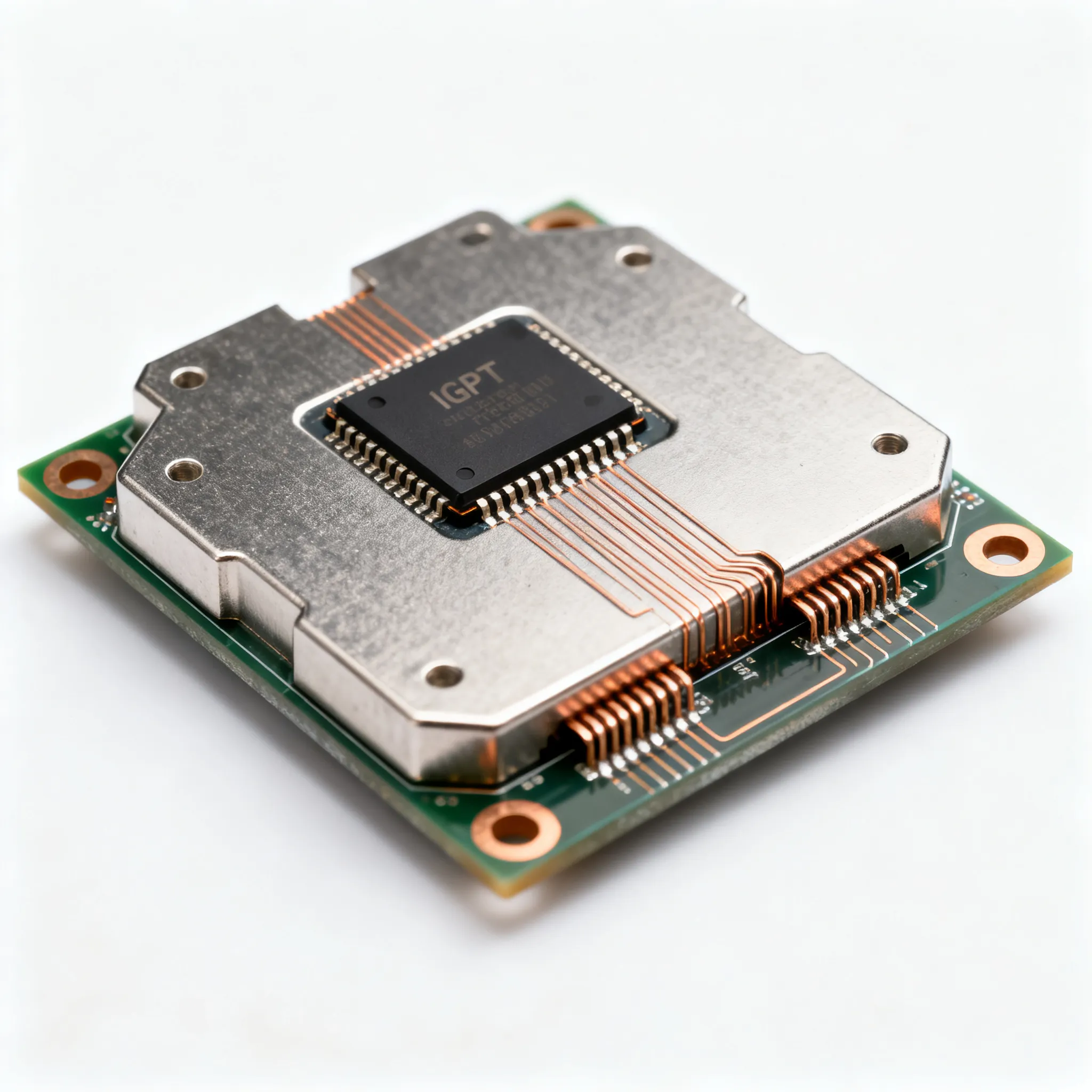
Power MOSFETs (Metal-Oxide-Semiconductor Field-Effect Transistors) are critical components used for switching and amplifying electronic signals in various applications. Unlike their bipolar counterparts, MOSFETs offer high input impedance and fast switching speed, making them ideal for modern electronic circuits. The key parameters to understand in MOSFET datasheets include the threshold voltage (VGS(th)), drain-to-source voltage (VDS), continuous drain current (ID), and on-resistance (RDS(on)). These parameters determine the MOSFET's suitability for specific applications, influencing everything from efficiency to thermal management.
Understanding the core principles of MOSFET operation is essential. The gate voltage controls the conduction state, which allows for efficient switching. The threshold voltage indicates the minimum gate-source voltage required to turn the MOSFET on. The drain-to-source voltage represents the maximum voltage the MOSFET can handle in the off state, while the continuous drain current specifies the maximum current it can conduct in the on state. The on-resistance is crucial for efficiency, as it affects the power loss during operation. These parameters, along with thermal and mechanical specifications, form the basis of any comprehensive datasheet analysis.
Detailed Specifications
| Parameter | Value | Units | Notes |
|---|---|---|---|
| VDS - Drain-Source Voltage | 100 | V | Maximum voltage across drain-source |
| ID - Continuous Drain Current | 20 | A | Maximum continuous current flow |
| RDS(on) - On-Resistance | 0.05 | Ω | Resistance when MOSFET is on |
| VGS(th) - Gate-Source Threshold Voltage | 2.5 | V | Minimum voltage to turn on the MOSFET |
| PD - Power Dissipation | 50 | W | Maximum power the MOSFET can dissipate |
| Qg - Total Gate Charge | 25 | nC | Charge required to turn on the MOSFET |
| ton - Turn-On Time | 10 | ns | Time taken to turn on the MOSFET |
| toff - Turn-Off Time | 15 | ns | Time taken to turn off the MOSFET |
| Input Capacitance (Ciss) | 1000 | pF | Capacitance between gate and source |
| Output Capacitance (Coss) | 300 | pF | Capacitance between drain and source |
| Reverse Transfer Capacitance (Crss) | 50 | pF | Capacitance between gate and drain |
Thermal & Mechanical Specs
| Parameter | Value | Units | Notes |
|---|---|---|---|
| Junction-to-Ambient Thermal Resistance (RθJA) | 62 | °C/W | Thermal resistance from junction to ambient |
| Junction-to-Case Thermal Resistance (RθJC) | 1.5 | °C/W | Thermal resistance from junction to case |
| Maximum Junction Temperature (TJ) | 175 | °C | Maximum allowable junction temperature |
| Storage Temperature Range (TSTG) | -55 to 150 | °C | Temperature range for safe storage |
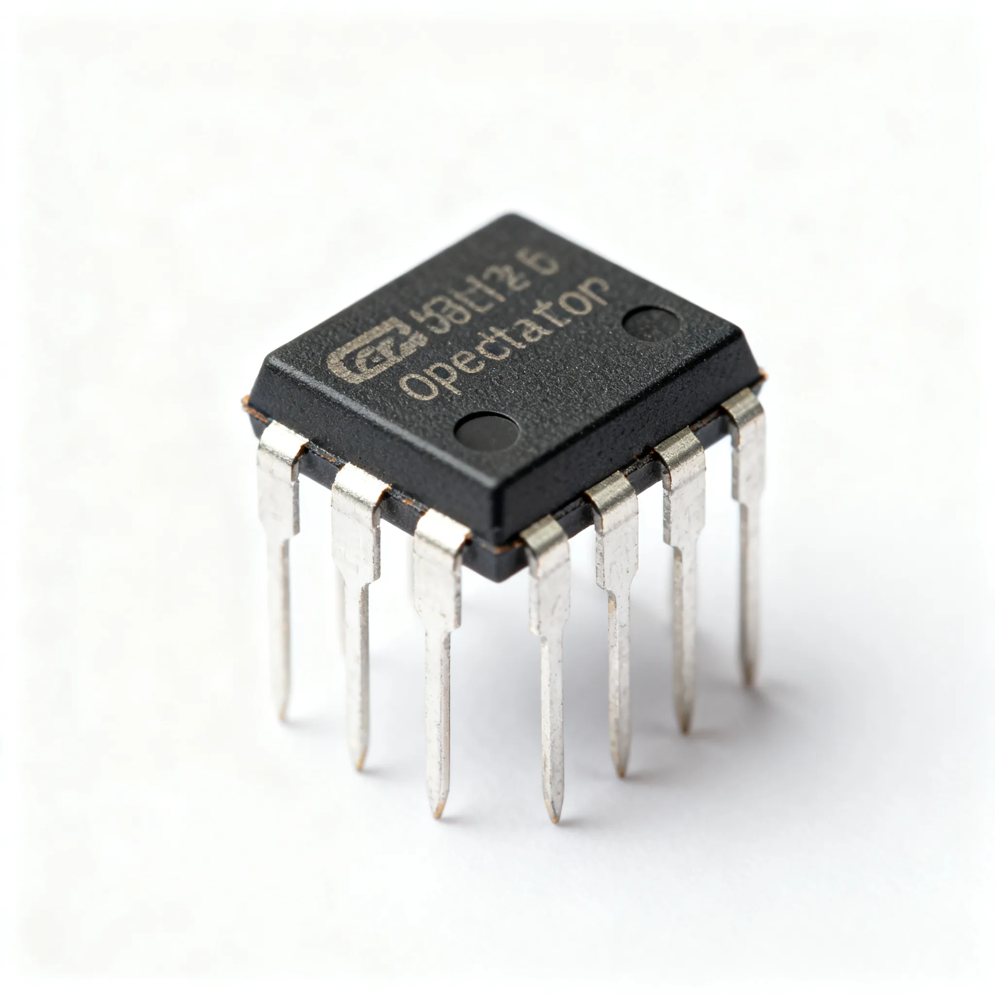
| Package Type | TO-220 | N/A | Standard package for power MOSFETs |
| Mounting Type | Through Hole | N/A | Mounting method for PCB |
| Weight | 1.7 | g | Weight of the component |
| Lead Finish | Matte Tin | N/A | Finish type for leads |
Application Comparison
| Application | Recommended MOSFET | Key Parameters | Notes |
|---|---|---|---|
| DC-DC Converter | IRF3205 | VDS: 55V, ID: 110A | High efficiency for low voltage applications |
| Motor Control | IRF540 | VDS: 100V, ID: 33A | Suitable for medium power motors |
| Audio Amplifier | IRF630 | VDS: 200V, ID: 9A | Low distortion for audio applications |
| Solar Inverter | IRFP260N | VDS: 200V, ID: 50A | High power handling for solar applications |
| Switching Power Supply | IRF740 | VDS: 400V, ID: 10A | Reliable for high voltage power supplies |
The tables above provide a comprehensive overview of the electrical, thermal, and application-specific parameters critical to selecting the right MOSFET for your design. Each parameter plays a vital role in ensuring that the MOSFET can handle the operational demands of your application, whether it be in high-frequency switching, power conversion, or thermal management.
Design Considerations
When designing circuits with power MOSFETs, several considerations must be kept in mind to ensure optimal performance. First, the selection of a MOSFET should align with the application's voltage and current requirements. For instance, choosing a MOSFET with a higher VDS than the application's maximum voltage ensures reliability. Similarly, the continuous drain current (ID) must exceed the application's peak current to prevent thermal overload.
Thermal management is another critical aspect of MOSFET design. The junction-to-ambient (RθJA) and junction-to-case (RθJC) thermal resistances provide insights into the component's heat dissipation capabilities. Effective heat sinking and adequate ventilation are essential to maintain the junction temperature below the maximum allowable limit.
The on-resistance (RDS(on)) directly affects the efficiency of the MOSFET. Lower on-resistance translates to reduced power loss and heat generation, making it a crucial parameter for high-efficiency designs. Additionally, the gate charge (Qg) and switching times (ton and toff) determine the speed at which the MOSFET can switch, impacting the overall performance in high-frequency applications.
Lastly, consider the package type and mounting method, as these influence the mechanical stability and ease of integration into the circuit. Through-hole packages like TO-220 offer robust mechanical support, while surface-mount packages provide compactness for space-constrained designs.
Step-by-Step Guide
- Define Application Requirements: Start by identifying the voltage, current, and switching frequency requirements of your application. This will help narrow down the list of suitable MOSFETs.
- Examine Electrical Specifications: Refer to the electrical specifications table to select a MOSFET with appropriate VDS, ID, and RDS(on) values. Ensure these parameters meet or exceed your application needs.
- Assess Thermal Management Needs: Calculate the power dissipation using the formula P = ID² * RDS(on). Ensure adequate heat sinking based on the thermal resistance values provided in the datasheet.
- Evaluate Switching Performance: Check the gate charge (Qg) and switching times (ton and toff) to ensure the MOSFET can handle the desired switching speed and frequency.
- Consider Package and Mechanical Constraints: Choose a package type that fits your PCB layout and mechanical constraints. Ensure the mounting method aligns with your assembly process.
- Prototype and Test: Build a prototype circuit and test the MOSFET under real operating conditions. Measure parameters such as efficiency, thermal performance, and switching behavior to verify the design.
- Iterate and Optimize: Based on test results, iterate on the design to optimize performance. This may involve selecting different MOSFETs, adjusting circuit parameters, or enhancing thermal management.
- Document the Design: Once the design is finalized, document all specifications, test results, and design decisions for future reference and manufacturing.
Common Issues & Solutions
- Overheating: If the MOSFET is overheating, check the thermal management and ensure adequate heat sinking. Consider selecting a MOSFET with lower RDS(on) or improving ventilation.
- Insufficient Switching Speed: If the circuit is not switching fast enough, verify the gate charge and drive capability of the gate driver circuit. A MOSFET with lower Qg may be necessary.
- Excessive Power Loss: High power loss can be mitigated by selecting a MOSFET with lower on-resistance and optimizing the drive circuit to reduce switching losses.
- Voltage Spikes: Voltage spikes can occur during switching. Use snubber circuits or TVS diodes to protect the MOSFET from overvoltage conditions.
- Gate Oscillations: If gate oscillations are observed, check the gate drive circuit for impedance mismatches and add gate resistors or ferrite beads to dampen oscillations.
Applications & Use Cases
Power MOSFETs are integral to a wide range of applications. In DC-DC converters, MOSFETs like the IRF3205 are used for their high efficiency and fast switching capabilities. Motor control applications benefit from MOSFETs such as the IRF540, which provide reliable performance for medium power motors. In audio amplifiers, the IRF630 offers low distortion for high-fidelity sound reproduction. Solar inverters and switching power supplies also rely on MOSFETs like the IRFP260N and IRF740 for their high power handling and voltage tolerance.
Selection & Sourcing Guide
Selecting the right MOSFET involves balancing electrical, thermal, and mechanical specifications to meet application requirements. Sourcing these components from reliable distributors ensures quality and availability. For a comprehensive selection of MOSFETs, visit IC Online to explore a wide range of options and secure competitive pricing and fast delivery.
FAQ
- What is the significance of the VGS(th) parameter? The gate-source threshold voltage indicates the minimum voltage required to turn on the MOSFET. It is crucial for ensuring the MOSFET operates within the desired range.
- How do I calculate the power dissipation of a MOSFET? Power dissipation can be calculated using P = ID² * RDS(on), where ID is the drain current and RDS(on) is the on-resistance.
- Why is thermal management important for MOSFETs? Proper thermal management prevents overheating, ensuring the MOSFET operates efficiently and prolonging its lifespan.
- What role does gate charge play in MOSFET performance? Gate charge affects the switching speed of the MOSFET. Lower gate charge allows for faster switching, which is important in high-frequency applications.
- How can I prevent voltage spikes in my circuit? Use snubber circuits or transient voltage suppressors (TVS) to protect the MOSFET from voltage spikes during switching.
- What is the difference between RθJA