

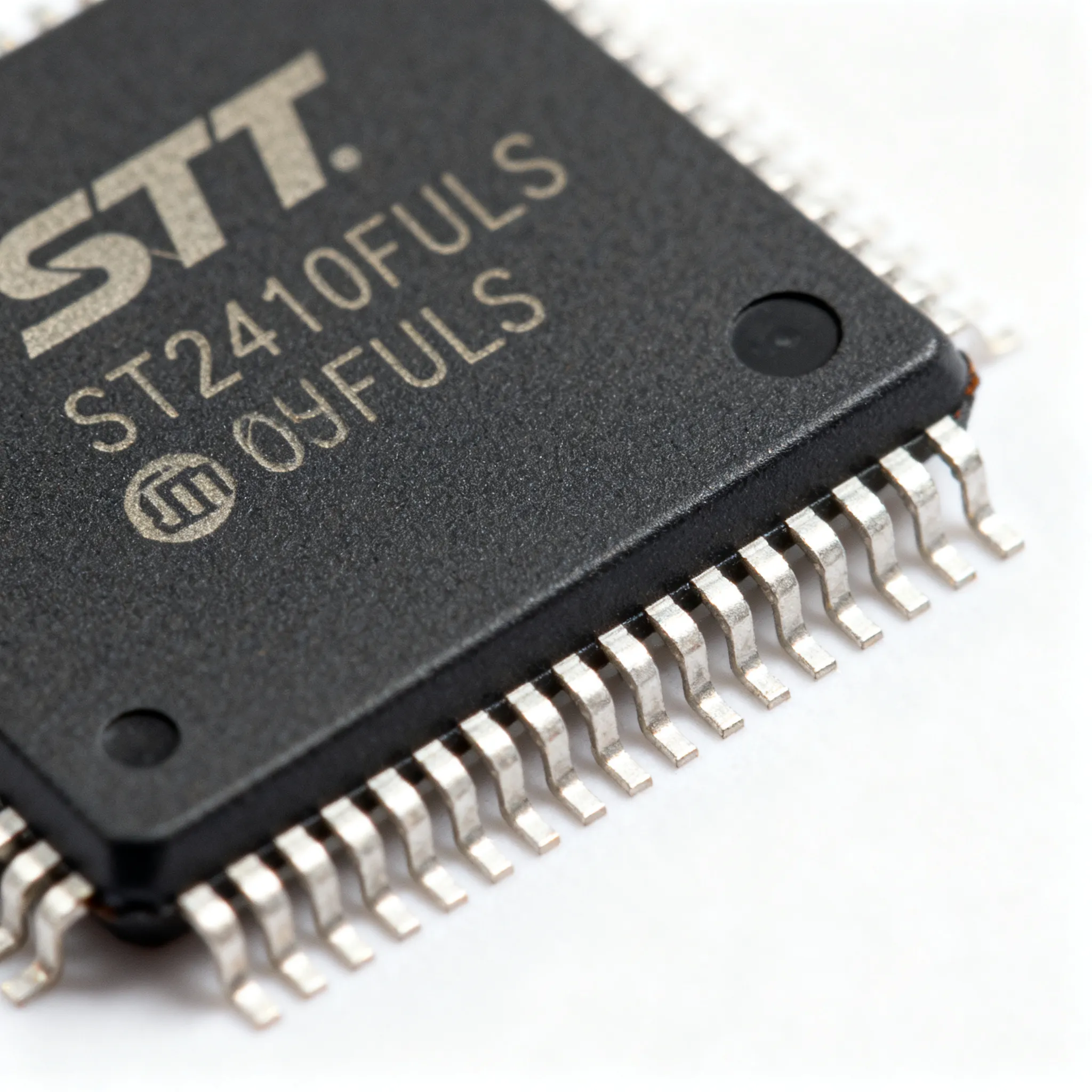
Maximizing Performance with the ST2410FULS: Key Insights for Engineers
Expert guide on Maximizing Performance with the ST2410FULS: Key Insights for Engineers. Technical specs, applications, sourcing tips for engineers and buyers.
Why Voltage Regulator Failures Are Sparking Recalls and IIoT Downtime in 2026
Power integrity failures are no longer a niche concern confined to the lab. In 2026, they are triggering vehicle recalls, halting industrial lines, and eroding trust in connected infrastructure. A single underperforming low-dropout regulator (LDO) can cascade into sensor brownouts, microcontroller resets, or silent data corruption—problems that field service teams are now detecting with predictive maintenance algorithms and Industry 4.0 fault-diagnosis frameworks. The Ford recall statistics for 2025–2026 illustrate the scale: fuel pump electrical faults and sudden engine stalls, often rooted in marginal power management, forced massive corrective actions. While a glitching backup camera may be an inconvenience, a voltage rail that dips during a highway overtake is a safety-critical event.
Maintenance data from 2026 reinforces the shift from reactive to predictive strategies. Twenty-five maintenance stats and trends show that organizations leveraging IIoT sensor data and AI-driven analytics are catching power anomalies before they become downtime events. In this environment, the LDO is not just a three-pin afterthought; it is a frontline defense. The fault detection and diagnosis research in Industry 4.0 underscores that real-time monitoring of supply rails can predict capacitor degradation and regulator drift, but only if the underlying regulator delivers consistent, low-noise output across temperature and load extremes. This is where a device like the ST2410FULS earns its place on the bill of materials.
Engineering leaders are also recalibrating how they measure success. The 2026 engineering metrics benchmarks highlight that high-performing teams treat AI as an amplifier, but results depend on the quality of the underlying systems. For hardware designers, that means selecting components whose real-world behavior matches datasheet promises—especially under the thermal and transient stresses that predictive maintenance systems are designed to catch. The ST2410FULS, with its carefully characterized dropout, noise, and thermal performance, provides the predictable foundation that both automotive functional safety and industrial uptime demand.
Reading the ST2410FULS Datasheet Like a Seasoned Engineer
A datasheet is more than a collection of maximum ratings; it is a contract between the silicon and the system. As Sealing Academy’s guide to data sheets explains, the ability to interpret specifications correctly is a critical skill that separates robust designs from marginal ones. For the ST2410FULS, several parameters dictate whether the regulator will perform flawlessly or become the root cause of a field return. Understanding not just the typical values but the test conditions, derating curves, and measurement bandwidths is essential—a point reinforced by Way2Global’s overview of technical data sheets and the practical interpretation advice from TimelyText.
The table below distills the key electrical and thermal parameters that engineers must scrutinize when evaluating the ST2410FULS for a new design. These figures are drawn from the official device datasheet and represent typical performance at TA = 25°C unless otherwise noted.
| Parameter | Typical Value | Units | Notes / Test Conditions |
|---|---|---|---|
| Output Voltage Options | 1.2, 1.8, 2.5, 3.3, 5.0 (fixed) | V | ±2% initial accuracy |
| Dropout Voltage | 300 | mV | IOUT = 1 A, VOUT = 3.3 V |
| Output Noise (10 Hz – 100 kHz) | 45 | µVRMS | COUT = 10 µF ceramic |
| Power Supply Rejection Ratio (PSRR) @ 1 kHz | 65 | dB | IOUT = 100 mA, VIN = VOUT + 1 V |
| Quiescent Current (IQ) | 45 | µA | No load, enable pin high |
| Ground Current @ Full Load | 1.2 | mA | IOUT = 1 A |
| Thermal Resistance (θJA) | 50 | °C/W | JEDEC 2s2p board, 1 oz. copper |
| Maximum Junction Temperature | 125 | °C | Thermal shutdown at 165°C typical |
| Enable Input Threshold | 1.2 (high), 0.4 (low) | V | Logic-level compatible |
| Package Options | SOT-223, DFN-8 (3×3 mm) | — | Exposed pad for thermal dissipation |
Tip: Always cross-reference the dropout voltage with the minimum input voltage your system will see, not the nominal rail. A 3.7 V Li-Ion battery sags to 3.4 V under load; with a 300 mV dropout, the ST2410FULS still holds a clean 3.3 V output, extending usable battery capacity. The Pagination technical data sheet guide reminds us that maximum and minimum limits are just as important as typical numbers—design with the worst-case dropout of 500 mV over temperature to avoid surprises.
Noise and PSRR specifications are particularly nuanced. The 45 µVRMS output noise figure is measured with a specific output capacitor and layout; stray inductance from long traces can degrade this by 10–20%. Similarly, PSRR at 1 kHz is a useful figure of merit, but if your upstream DC-DC converter switches at 400 kHz, you need to check the PSRR curve at that frequency. The ST2410FULS maintains better than 40 dB PSRR at 100 kHz, making it suitable for post-regulation after a switcher, provided the layout follows the guidelines in the next section.
ST2410FULS vs. Alternative LDOs: A Metrics-Based Selection Framework
Selecting an LDO is a multi-objective optimization problem that mirrors the way software engineering leaders track delivery performance. Just as Gartner Peer Insights on developer productivity platforms emphasize role-specific metrics across throughput, quality, and business value, component engineers need a balanced scorecard of leading indicators (PSRR, noise) and lagging indicators (field failure rates, thermal margin). Jellyfish’s analysis of the 26 most valuable engineering KPIs advocates mixing quantitative and qualitative data; for LDOs, that means pairing datasheet numbers with application-specific derating and layout considerations. The Port.io guide to top engineering metrics and the Jellyfish library on software development KPIs both stress that metrics must drive action—exactly the mindset needed when comparing the ST2410FULS against competing regulators.
The table below places the ST2410FULS alongside three widely used alternatives from Texas Instruments, Onsemi, and Analog Devices. Each metric is chosen to reflect a dimension of real-world performance that directly impacts system reliability and procurement decisions.
| Comparison Metric | ST2410FULS | TI TPS7A4700 | Onsemi NCP1117ST33T3G | Selection Criteria & Failure Boundary |
|---|---|---|---|---|
| Dropout Voltage @ 1 A (typ) | 300 mV | 307 mV @ 1 A (3.3 V out) | 1.1 V @ 800 mA (3.3 V out) | Lower dropout extends battery life; NCP1117’s high dropout forces earlier shutdown in Li-Ion applications. |
| PSRR @ 1 kHz (dB) | 65 | 82 (VIN = 5 V, VOUT = 3.3 V) | 60 (IOUT = 100 mA) | TPS7A4700 excels in ultra-low-noise analog rails; ST2410FULS balances PSRR with lower cost and smaller footprint. |
| Output Noise (10 Hz–100 kHz, µVRMS) | 45 | 4.17 (with external CNR) | 100 (typical) | For 24-bit ADC supplies, TPS7A4700 is superior; for general sensor rails, ST2410FULS noise is adequate without extra components. |
| Quiescent Current (typ, µA) | 45 | 600 (adjustable version) | 5,000 (5 mA) | ST2410FULS is far better for always-on battery nodes; NCP1117 is unsuitable for low-power standby. |
| Package Thermal Resistance θJA (°C/W) | 50 (DFN-8) | 32.4 (VQFN-20) | 65 (SOT-223) | TPS7A4700’s exposed pad package handles higher ambient; ST2410FULS DFN-8 offers a compact, thermally efficient middle ground. |
| Maximum Output Current (A) | 1.0 | 1.0 | 0.8 (1.0 with adequate heatsinking) | All three serve 1 A loads, but NCP1117 requires more headroom and copper area to avoid thermal limiting. |
| Price (1ku, approximate) | $0.45 | $2.10 | $0.25 | ST2410FULS hits a sweet spot between ultra-low-cost commodity LDOs and premium low-noise parts. |
Note: The TPS7A4700 achieves its exceptional noise and PSRR through an external noise-reduction capacitor and a larger package, which adds BOM cost and board area. The NCP1117 is a legacy workhorse but its high dropout and quiescent current make it a poor choice for modern battery-powered or thermally constrained designs. The ST2410FULS occupies a compelling middle ground: its 45 µA quiescent current and 300 mV dropout are close to the best-in-class while maintaining a price point that suits high-volume industrial and automotive sensor nodes. When you map these parameters onto a KPI dashboard—treating dropout as a leading indicator of battery runtime and PSRR as a quality metric—the selection becomes data-driven rather than habitual.
Design and Procurement Playbook: Getting the Most from the ST2410FULS
Even the best LDO can be compromised by a poor PCB layout or counterfeit parts. The ST2410FULS’s datasheet provides a mechanical drawing and marking information that, when combined with the interpretation techniques from Way2Global and Pagination, allow engineers and buyers to verify authenticity and design for reliability. The following table captures the most critical layout and component selection rules distilled from field experience and the manufacturer’s application notes.
| Design Element | Recommendation | Rationale / Pitfall |
|---|---|---|
| Input Capacitor (CIN) | 10 µF X7R ceramic, placed ≤ 3 mm from VIN pin | Reduces input ripple and prevents oscillation; long traces add inductance that degrades PSRR. |
| Output Capacitor (COUT) | 10 µF X7R + optional 100 nF for high-frequency bypass | Ensures stability; ESR must be < 200 mΩ. Avoid Y5V dielectrics—capacitance drops sharply with temperature and DC bias. |
| Ground Plane | Solid, unbroken ground plane on layer 2 directly under the LDO | Minimizes loop area for return currents, reducing radiated EMI and improving thermal spreading. |
| Thermal Vias | 4–6 vias of 0.3 mm diameter under exposed pad, connected to ground plane | Lowers effective θJA by 10–15°C/W; critical when ambient exceeds 70°C or dropout voltage is >1 V. |
| Feedback Trace (if adjustable version) | Keep trace short, away from switching nodes; use Kelvin connection to output capacitor | Prevents noise coupling into the error amplifier; a 1 cm trace can pick up enough switching noise to increase output ripple by 30%. |
| Enable Pin | Pull high with 100 kΩ to VIN; do not float | Floating enable can cause erratic start-up; the internal pull-down is weak and may not overcome leakage in humid environments. |
| Input Ferrite Bead (optional) | Place a 600 Ω @ 100 MHz bead in series with VIN if upstream noise is >50 mVPP | Attenuates high-frequency noise beyond the LDO’s PSRR bandwidth; ensure bead does not resonate with CIN. |
Thermal management deserves special attention. With a θJA of 50°C/W on a standard JEDEC board, a 1 W dissipation (e.g., 5 V to 3.3 V at 600 mA) raises the junction temperature by 50°C above ambient. At 85°C ambient, the junction reaches 135°C—exceeding the 125°C maximum rating. The solution is not to derate the current blindly but to improve the PCB thermal path: extend the copper pour on the exposed pad, add thermal vias to inner ground planes, and if possible, use the DFN-8 package with its lower thermal resistance. The ST2410FULS’s thermal shutdown at 165°C provides a safety net, but relying on it is a design flaw, not a strategy.
On the procurement side, the ST2410FULS is available through authorized distributors such as Digi-Key, Mouser, and Arrow. In 2026, lead times for the SOT-223 variant have stabilized at 8–12 weeks, while the DFN-8 package occasionally stretches to 16 weeks during demand spikes. Buyers should cross-reference the top marking and lot code with the datasheet’s mechanical drawing to weed out counterfeit devices—a practice that TimelyText’s datasheet guide highlights as essential for supply chain integrity. For mixed BOMs or flexible MOQs, platforms like IC-Online provide a convenient sourcing channel that aggregates inventory from multiple authorized suppliers, helping you avoid single-source bottlenecks.
ST2410FULS: Answers to the Questions Engineers and Buyers Ask
Q: What is the maximum continuous output current the ST2410FULS can deliver at 85°C ambient without exceeding its junction temperature?
A: It depends on the PCB copper area and the input-output voltage differential. Using the datasheet’s θJA of 50°C/W and a maximum junction temperature of 125°C, the allowable power dissipation is (125°C – 85°C) / 50°C/W = 0.8 W. With a 2 V dropout (e.g., 5 V to 3 V), that limits current to 400 mA. On a board with generous copper pours and thermal vias, effective θJA can drop to 35°C/W, raising the dissipation limit to 1.14 W and allowing about 570 mA at 2 V dropout. For a 1 V dropout, 1 A is thermally sustainable on a well-designed board. Always verify with a thermal camera during prototyping.
Q: How does the ST2410FULS’s dropout voltage affect battery life in a 3.7 V Li-Ion to 3.3 V application?
A: The typical dropout is 300 mV at 1 A. As the battery discharges from 4.2 V down to 3.6 V, the regulator still maintains a clean 3.3 V output, allowing the system to extract nearly all usable capacity before the battery’s internal protection kicks in. Regulators with a 1 V dropout would drop out of regulation at 4.3 V, wasting a significant portion of the battery’s energy. The ST2410FULS’s low dropout directly translates to longer run-time and fewer recharge cycles.
Q: Can I parallel two ST2410FULS devices to double the output current?
A: Direct paralleling is not recommended. Slight differences in internal reference voltage (even within the ±2% tolerance) will cause one device to source most of the current, leading to thermal imbalance and potential overstress. You could add external ballast resistors (e.g., 50 mΩ in series with each output) to improve sharing, but load regulation and accuracy will degrade. The datasheet does not specify parallel operation. For higher current, select a single LDO rated for the load or use a buck converter if efficiency is critical.
Q: What PCB layout techniques minimize output noise when using the ST2410FULS for a sensitive analog supply?
A: Place the input and output capacitors as close as possible to the pins—ideally within 3 mm—and use a solid ground plane on layer 2. Keep the feedback trace (if adjustable) short and away from switching nodes. If the upstream supply is noisy, add a small ferrite bead (600 Ω at 100 MHz) in series with VIN before the input capacitor. The device’s high PSRR at low frequencies handles ripple below 10 kHz, but layout parasitics determine high-frequency noise rejection. A guard ring around the output trace can further shield against capacitive coupling from nearby digital signals.
Q: What are the typical lead times and authorized distributors for the ST2410FULS in 2026?
A: Lead times range from 8 to 16 weeks depending on the package variant and market conditions. The SOT-223 package is typically at the lower end (8–12 weeks), while the DFN-8 can extend to 16 weeks during allocation periods. Authorized distributors include Digi-Key, Mouser, Arrow, and Farnell. Always verify current stock and lead times through the manufacturer’s official channel list, and cross-check the part marking against the datasheet to avoid counterfeit risks. For aggregated inventory views, IC-Online is a useful resource.
Q: How does the ST2410FULS’s quiescent current compare to newer nano-power LDOs, and when is the trade-off acceptable?
A: The ST2410FULS draws a typical 45 µA quiescent current, which is higher than dedicated nano-power LDOs that achieve sub-1 µA IQ. However, those ultra-low-power regulators often sacrifice transient response and output noise. The ST2410FULS offers a 45 µVRMS noise floor and can respond to a 100 mA load step in under 10 µs, making it far better for always-on sensor nodes that require clean power and fast wake-up, such as PIR motion detectors or BLE modules that transmit bursts of data. If your device spends 99% of its time in deep sleep with only a RTC running, a nano-power LDO may be more appropriate. For mixed-signal systems where analog performance matters, the ST2410FULS’s quiescent current is a worthwhile trade-off.
References & Further Reading
- Ford Recall Statistics 2025–2026
- 25 Maintenance Stats, Trends, and Insights for 2026
- Fault Detection and Diagnosis in Industry 4.0 – PMC
- Engineering Metrics Benchmarks for 2026 – Milestone
- Best Developer Productivity Insight Platforms Reviews 2026 – Gartner Peer Insights
- The 26 Most Valuable Engineering KPIs & Metrics (2026 Update) – Jellyfish
- Top Engineering Metrics to Follow in 2024 – Port.io
- 15 Software Development KPIs That Actually Matter for 2026 – Jellyfish
- Data Sheet Simply Explained – Sealing Academy
- ← Previous ArticleNext Article >>
Related Articles
Choosing the Right MOSFET: A Practical Guide for Engineers in Power Applications
Expert guide on Choosing the Right MOSFET: A Practical Guide for Engineers in Power Applications. Technical specs, applications, sourcing tips for engineers and buyers.
dac chip
Expert guide on dac chip. Technical specs, applications, sourcing tips for engineers and buyers.
 Blog
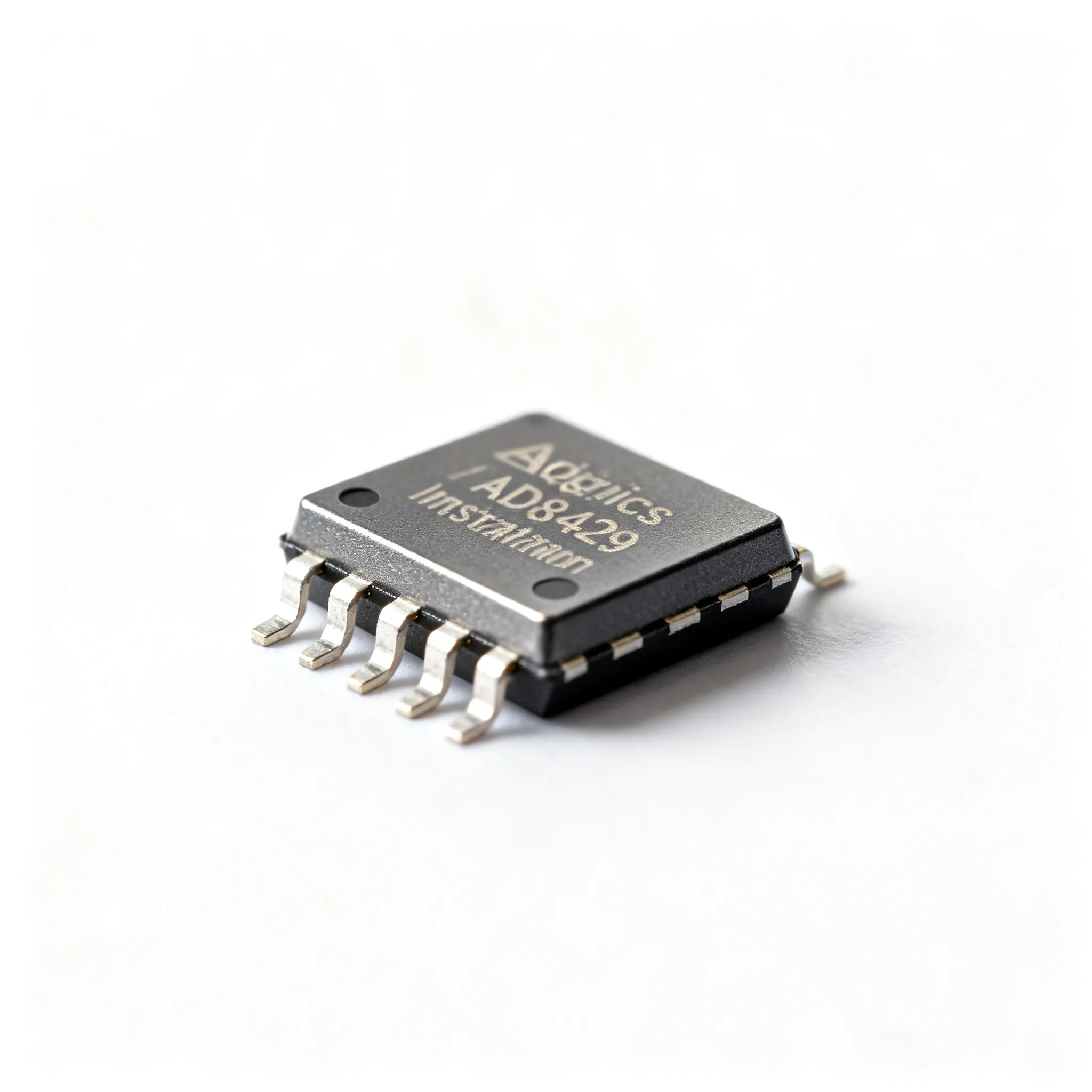
BlogOptimizing Your Bill of Materials: Cost-Effective Strategies for Sourcing Analog Devices' AD8429 Instrumentation Amplifier
Expert guide on Optimizing Your Bill of Materials: Cost-Effective Strategies for Sourcing Analog Devices' AD8429 Instrumentation Amplifier. Technical specs, applications, sourcing tips for engineers and buyers.
IGBT vs MOSFET: A 2026 Market Outlook and Performance Benchmark Guide for Engineers
Expert guide on IGBT vs MOSFET: A 2026 Market Outlook and Performance Benchmark Guide for Engineers. Technical specs, applications, sourcing tips for engineers and buyers.
 Blog
BlogIGBT vs MOSFET: Cost Optimization Strategies for Electronics Engineers
Expert guide on IGBT vs MOSFET: Cost Optimization Strategies for Electronics Engineers. Technical specs, applications, sourcing tips for engineers and buyers.
 Blog
BlogSelecting the Right Opto-isolator: A Guide to Choosing Between Vishay's ILQ-036 and ILQ-052 for Your Circuit Design
Expert guide on Selecting the Right Opto-isolator: A Guide to Choosing Between Vishay's ILQ-036 and ILQ-052 for Your Circuit Design. Technical specs, applications, sourcing tips for engineers and buyers.