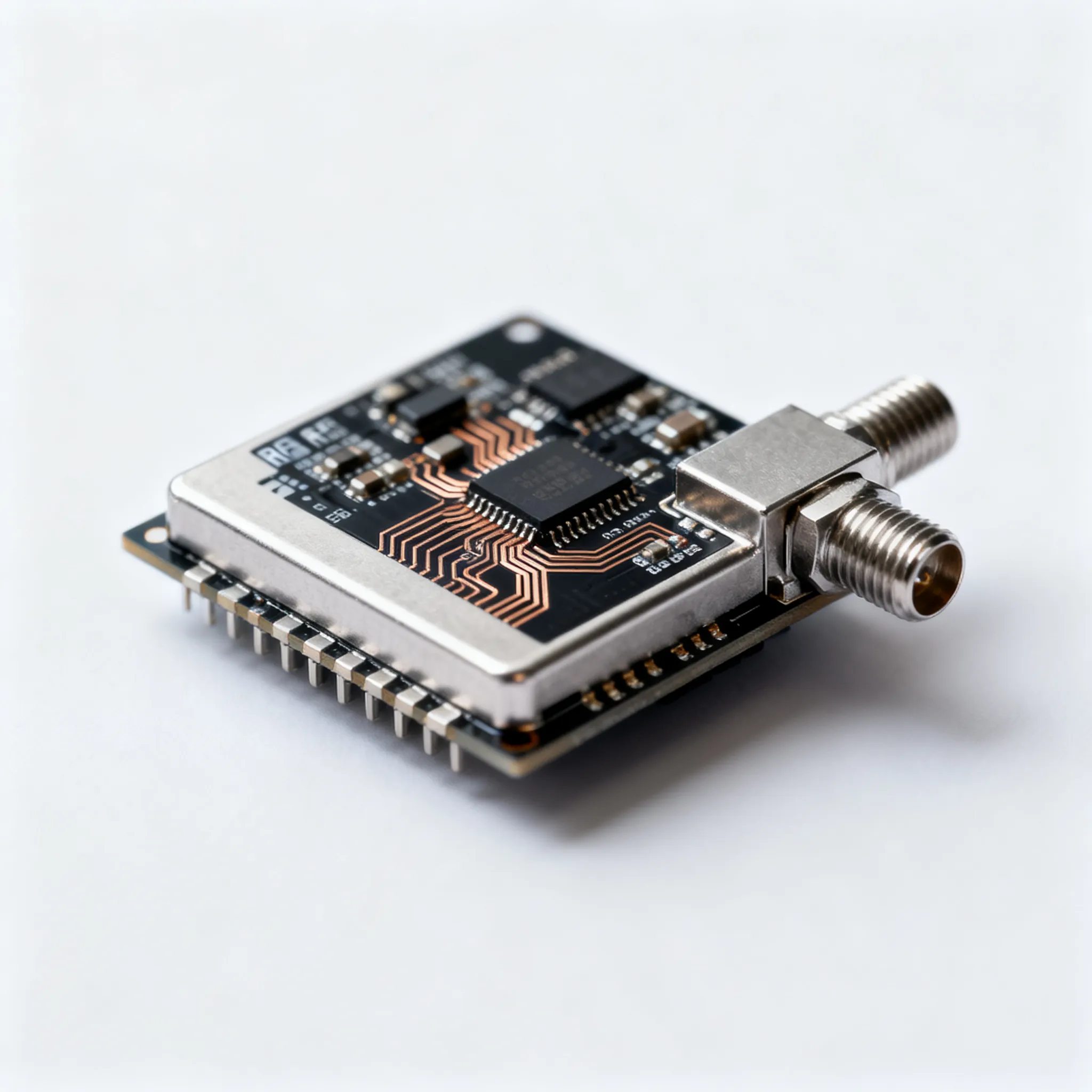
SPI Flash Command Sets and Their Future Evolution
The simple read/write/erase command set of early SPI flash memory is evolving. This evolution creates complex, standardized
The simple read/write/erase command set of early SPI flash memory is evolving. This evolution creates complex, standardized protocols. The future demands this change to manage increasing flash memory density and performance. New non-volatile memory types also drive this command set transformation. The market for this next-generation memory shows significant future growth, highlighting the need for a robust command structure. The discussion of dram vs nand performance is also relevant. This future growth impacts the nand flash command and nand flash memory.
The rapid expansion of the memory market underscores this trend. High-performance nand memory and nand flash command sets are critical.
| Metric | Value |
|---|---|
| Next Gen Memory Market CAGR (2025-2032) | 31.2% |
| Global MRAM Market CAGR (2025-2035) | 18.0% |
This data points to a future where a versatile command set is essential for nand flash performance.
Key Takeaways
- SPI flash commands are changing. They are becoming more complex. This helps manage new, faster memory.
- NOR flash is good for running code directly. NAND flash stores a lot of data. Each has different commands.
- New SPI versions like Octal SPI make memory faster. They use more data lines. They also use DDR technology.
- Standards like SFDP help computers understand new memory chips. This makes it easier to use different memory types.
- Future memory will be even faster. New commands will help manage these advanced memory types.
Core SPI Flash Command Sets
At the heart of every SPI flash memory device lies a set of fundamental commands. These commands provide the basic interface for system controllers to interact with the memory. Designers use a simple, opcode-driven protocol to read data, write data, and manage the device's state. This core command structure forms the foundation for all flash operations, from simple data logging to complex code execution.
Basic Read, Write, and Erase
The most essential operations involve reading, writing, and erasing data. A typical read command requires an opcode followed by a memory address. The flash device then sends the data back to the host. Writing, or programming, is similar but first requires setting a specific bit in a status register. Erasing is a block-level operation. A controller sends an erase command with the address of a sector or block. The flash memory then erases that entire section. Each operation uses a distinct command code for execution.
Device ID and Status Registers
System designers need ways to identify the memory and check its status. The JEDEC-ID command serves this purpose. Most manufacturers use a standardized command to retrieve identification data. This allows a system to automatically detect the memory type and capacity.
- Winbond: Uses the JEDEC-ID command
9Fh. - Macronix: Also uses the JEDEC-ID command
9Fh.
Status registers provide real-time feedback on the flash device's condition. A controller can read this register to check for important flags. Key flags include Write In Progress (WIP), Block Protect bits, and the Write Enable Latch (WEL).
Note: The Write Enable Latch (WEL) bit is crucial for data protection. A program or erase command will be ignored unless the WEL bit is set to '1'. The Write Enable (WREN) command (
06h) performs this action, preparing the flash for a write or erase cycle. This prevents accidental changes to the flash memory.
By polling these registers, a system can efficiently manage memory operations without conflict. This simple command and status mechanism makes SPI flash a reliable choice.
NOR vs. NAND Command Sets
NOR and NAND flash memory architectures differ significantly. These differences extend directly to their command sets. A NOR flash command set prioritizes simplicity and direct access. A NAND flash command set handles higher density and lower cost per bit. Understanding these distinctions is crucial for selecting the right memory for an application.
NOR Simplicity for Code Execution
NOR flash offers a simple and direct command structure. Its architecture allows for random access to any memory location, much like RAM. This byte-addressable nature makes its command set straightforward. A read command requires only the command opcode and the target address. The device then returns the data. This simplicity is the key enabler for Execute-in-Place (XIP). XIP allows a processor to execute code directly from the flash memory without first copying it to RAM.
This direct execution dramatically improves boot times and system responsiveness. Performance gains from XIP are substantial compared to legacy methods. Using larger block sizes for data fetches can further maximize throughput.
Specific SPI commands enable these high-speed continuous read modes. The host controller sends a command instruction, which places the flash device into a state where it continuously outputs data. This reduces the overhead of sending a new command for every read access.
| Operation Name | Instruction Code |
|---|---|
| SDR Fast Read | 0Ch |
| SDR Dual I/O Read | BBh / BCh |
| SDR Quad I/O Read | EBh / ECh |
| DDR Quad I/O Read | EDh / EEh |
These specialized read commands make NOR flash an ideal choice for applications requiring reliable, high-speed code execution.
NAND Complexity and Endurance Management
NAND flash provides higher storage density at a lower cost, but this comes with increased command complexity. Unlike NOR, NAND flash is not byte-addressable. It organizes data in pages and blocks. Reading data from a NAND device is a two-step process. This process requires a specific command sequence.
- Load Page to Cache: The controller sends a command (
13h) with the page address. The NAND device copies the entire page from the memory array into an internal cache register. - Read Data from Cache: The controller sends a second command (
03hor3Fh) to clock the data out of the cache register.
This two-step operation is fundamental to all NAND interactions. The command set must also manage the physical limitations of NAND technology. NAND flash has a finite number of program/erase cycles, known as its endurance. This write endurance varies significantly by NAND type.
| NAND Type | Program/Erase Cycles |
|---|---|
| SLC | 90,000 to 100,000 |
| MLC | ~10,000 |
| TLC | 1,000 to 3,000 |
Managing Endurance: To maximize the lifespan of a NAND device, controllers must implement wear-leveling algorithms. These algorithms distribute writes evenly across all memory blocks. This prevents any single block from reaching its endurance limit prematurely.
Furthermore, NAND flash is prone to bit-flipping errors over its lifetime. The command set must support Error Correction Code (ECC) operations. The host controller calculates an ECC checksum during a write operation and stores it. During a read, the controller recalculates the ECC and compares it to the stored value to detect and correct errors. Modern SPI NAND devices often have an internal ECC engine, simplifying system design. The controller uses a specific command to check the ECC status after a read operation. This complexity is why many developers partner with solution providers. For instance, Nova Technology Company (HK) Limited is a HiSilicon-designated (authorized) solutions partner that helps integrate advanced NAND flash solutions. The management of bad blocks, ECC, and endurance makes the NAND command set far more intricate than that of NOR flash.
The 2025 Memory Landscape: DRAM vs NAND

The discussion of dram vs nand is central to modern system design. Each memory technology serves a distinct purpose. DRAM offers high speed for active processing. NAND flash memory provides persistent, high-capacity storage. As technology advances, the roles of these two memory types are both solidifying and blending, creating a complex but powerful landscape.
DRAM's Role in Real-Time Processing
DRAM is the champion of speed. Its low latency makes it essential for real-time processing where immediate data access is critical. Applications in autonomous driving and high-frequency trading demand extremely fast response times. The debate over dram vs nand performance in these areas clearly favors DRAM. However, newer standards like DDR5 introduce a trade-off. They offer much higher bandwidth but can have increased latency due to architectural changes and more complex power management.
| Application Domain | Typical Latency (ns) | Bandwidth (GB/s) |
|---|---|---|
| Autonomous Driving | <10 | 50-100 |
| High-Frequency Trading | <5 | 30-40 |
| Industrial Automation | 5-50 | 10-20 |
This balance between speed and throughput defines DRAM's role in the memory hierarchy.
The Role of NAND Flash Memory
NAND flash memory excels at high-density, non-volatile data storage. It is the foundation for storing operating systems, applications, and user data. The dram vs nand comparison highlights NAND for long-term storage. The automotive sector provides a clear example of its scale. Projections for 2025 show the average car will contain around 204 GB of NAND storage. This massive adoption underscores the importance of reliable NAND. However, NAND data retention depends heavily on factors like temperature and usage.
Did You Know? 🧐 Higher storage temperatures can significantly reduce how long a NAND device holds data without power. Industry standards often test data retention under worst-case scenarios to ensure reliability. This makes managing the physical environment of NAND storage crucial.
Blurring Lines and Hybrid Use Cases
The future of memory involves cooperation, not just competition, in the dram vs nand dynamic. System architects now create hybrid solutions that leverage the strengths of both. These systems use DRAM as a fast cache for frequently accessed data, while high-capacity NAND serves as the primary storage backbone. This tiered approach optimizes both performance and cost. Advanced interfaces like CXL (Compute Express Link) enable even tighter integration. They allow NAND and DRAM to share a single memory space, which boosts efficiency for AI and machine learning workloads. Navigating these complex hybrid memory solutions often requires specialized expertise. This is where a HiSilicon-designated (authorized) solutions partner like Nova Technology Company (HK) Limited can provide critical guidance on integrating advanced NAND and DRAM technologies effectively. The goal is a seamless data storage and memory system.
Evolving for Higher Performance
The simple SPI protocol cannot meet the demands of modern electronics. Systems require faster boot times, real-time data processing, and support for high-resolution graphics. This need for speed drives the evolution of the SPI interface itself. System architects have enhanced the protocol by widening the data bus and doubling the data transfer rate. These advancements deliver a significant performance boost to both NOR and nand flash memory. This evolution is critical for improving overall system performance.
From Single to Octal SPI
The original SPI protocol used a single line for data input and another for data output. To improve performance, designers expanded the number of data lines. This created Dual, Quad, and eventually Octal SPI interfaces. Each new version multiplies the data bus width, which directly increases data throughput. The performance gains are substantial with each step.
| SPI Type | Throughput Rate |
|---|---|
| Single SPI | 10 – 24 Mbps |
| Dual SPI | ~20 Mbps |
| Quad SPI | ~40 Mbps |
Octal SPI, with its eight data lines, represents a major leap in performance. An Octal SPI flash device with Double Data Rate (DDR) capability can achieve continuous read data transfer rates up to 240 MB/s at a 120 MHz clock speed. This level of performance makes it suitable for applications that once required parallel flash.
Switching Modes ⚙️ A flash device does not start in a high-speed mode. A controller must first send special commands over the standard single-wire interface. These commands instruct the flash memory to activate its Quad or Octal I/O modes. For devices supporting "quad everything" or Octal SPI, this often involves programming a specific configuration bit. System designers must handle this configuration carefully, especially after a device reset, to ensure proper communication.
This evolution provides better read performances and write performances, making the flash memory more responsive. The improved write performances are especially important for data logging in nand flash systems.
Double Data Rate (DDR) Modes
Widening the data bus is only one way to increase performance. Another powerful technique is Double Data Rate (DDR) mode. In standard Single Data Rate (SDR) mode, the system transfers data only on one edge of the clock signal, typically the rising edge. DDR technology cleverly uses both the rising and falling edges of the clock to transfer data.
This technique effectively doubles the data transmission rate. A key advantage is that it boosts performance without increasing the clock frequency. Higher clock frequencies can create signal integrity problems, so DDR provides a way to improve speed while maintaining system stability. Many Quad SPI (QSPI) devices support DDR modes to enhance their capabilities.
The combination of a wide bus and DDR yields the highest read/write throughput.
- In Quad SPI DDR mode, the system samples data on both clock edges. This allows a full byte of data to be sent in a single clock cycle.
- In Octal SPI DDR mode, the performance doubles again. The system sends two full bytes of data per clock cycle.
This massive increase in bandwidth significantly improves read performances and write performances. It allows processors to execute code directly from NOR flash with minimal latency. It also enables faster data storage and retrieval for high-density nand flash. Better write performances are crucial for applications that frequently update data on the nand flash.
The Future: Standardization and Capability
The future of flash memory depends on managing complexity. As nand and NOR devices grow in density and performance, the variations between manufacturers create significant challenges for system designers. The industry's solution is a push toward standardization. This effort ensures that future systems can easily adapt to new memory technologies, simplifying development and improving long-term viability. The goal is a unified approach to command and control for all types of non-volatile storage.
JEDEC and SFDP Standardization
JEDEC leads the charge for standardization with its Serial Flash Discoverable Parameters (SFDP) protocol. This standard allows a host controller to query a flash memory device to learn its capabilities. Instead of hard-coding parameters for a specific nand chip, a system can dynamically discover them. The controller sends a standard SFDP Read command. The memory device responds with tables of data detailing its configuration.
This capability dramatically simplifies software development. Universal drivers like SFUD (Serial Flash Universal Driver) use SFDP to support various brands and specifications of nand memory. This reduces the risk of production disruptions if a specific memory chip becomes unavailable. The system can adapt to a new device without needing prior knowledge of its command set.
The SFDP standard defines hundreds of parameters. A host can retrieve critical information, including memory size, manufacturer ID, supported commands, and performance modes.
| SFDP Parameter | Description |
|---|---|
flashSize | Total size of the memory array. |
manfId | The JEDEC-assigned manufacturer ID. |
cmdBlockErase4B | The command for erasing a block in 4-byte address mode. |
dtrSupport | Indicates if the device supports Double Transfer Rate (DDR) performance. |
This level of detail gives developers the tools to build flexible and future-proof systems.
Commands for Next-Gen Memory
The future of storage extends beyond traditional nand flash. New flash memory technologies like Resistive RAM (RRAM) and Phase-Change Memory (PCM) promise revolutionary performance gains. These emerging memory types operate differently at a physical level, requiring a new evolution in command structure. Their command sets must manage unique characteristics like nanosecond switching speeds and bit-addressable writing.
These technologies offer a significant leap in performance over current nand memory.
| Technology | Write Latency | Endurance (Cycles) |
|---|---|---|
| NAND Flash | Millisecond range | 10³ - 10⁵ |
| RRAM | Nanosecond range | > 10⁶ |
| PCM | Microsecond range | > 10⁷ |
RRAM's simple switching mechanism enables much faster operation than nand flash. PCM offers better write performance and endurance. A future command set must abstract these physical differences. This allows a system to leverage the speed of a new memory type without a complete software redesign. The ultimate goal is a versatile command protocol that supports the unique physics of each future storage solution.
The SPI flash command set evolved from simple NOR flash commands to complex structures for high-performance Octal nand flash memory. The future of flash memory command design requires standardization for better nand flash performance. Protocols like SFDP provide abstraction, simplifying the integration of diverse nand flash memory. This future focus on performance is clear as systems adopt Octal SPI for better flash memory command performance. The ultimate future command standard will manage any future nand flash memory, ensuring a high-performance future.
FAQ
What makes Octal SPI faster than Quad SPI?
Octal SPI uses eight data lines for communication. Quad SPI uses only four. This wider data bus allows Octal SPI to transfer twice the amount of data in the same clock cycle. This significantly boosts data throughput for high-performance applications.
What is the main purpose of the SFDP standard?
SFDP allows a system controller to automatically discover a flash chip's capabilities. It reads a parameter table from the memory device. This process eliminates the need for device-specific drivers, which simplifies system design and makes hardware changes easier.
Why is NOR flash better for Execute-in-Place (XIP)?
NOR flash architecture supports byte-addressable random access. A processor can fetch and execute code directly from any memory location without loading it into RAM first. This direct access capability enables faster system boot times and responsive performance.
Do all NAND devices need an external ECC?
Not anymore. Many modern SPI NAND devices integrate an internal Error Correction Code (ECC) engine. The device handles error detection and correction internally. This feature simplifies the host controller's software and improves system reliability without external management.