How 3D Integrated Circuits Enable Smaller, Smarter Electronic Components
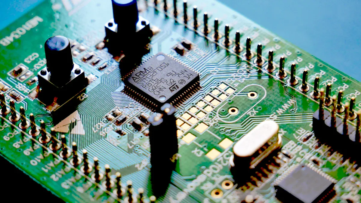
3D integrated circuits have changed how engineers make electronics. These circuits use vertical stacking and special packaging. This helps make devices smaller and work better. For example, 3D Mechatronic Integrated Devices can have conductor spacing as tiny as 150 µm.
3D integrated circuits have changed how engineers make electronics. These circuits use vertical stacking and special packaging. This helps make devices smaller and work better. For example, 3D Mechatronic Integrated Devices can have conductor spacing as tiny as 150 µm. This helps make electronic devices even smaller. 3D ICs have many active layers. These layers help mix automation, communication, and other features in small products. The table below shows how 3D packaging and integration help more people use electronics, IoT, and automation. This leads to faster communication and smarter machines.
|
Technology/Application Segment |
Market Share / Growth Metric |
Year / Period |
Performance/Adoption Insight |
|---|---|---|---|
|
3D Wafer-Level Chip-Scale Packaging (WLCSP) |
38.3% market share |
2023 |
Chosen for small size, lower cost, and good electrical performance in smartphones, tablets, and wearables |
|
3D Through-Silicon Via (TSV) |
Highest CAGR expected |
2024-2032 |
Growth comes from need for fast, high-performance apps that use vertical stacking and have less delay |
|
Memory (HBM, 3D NAND, stacked DRAM) |
34.3% market share |
2023 |
3D/2.5D packaging lets memory hold more, work better, and have less delay |
|
Consumer Electronics Segment |
33.7% market share |
2023 |
Leads the end-user group; devices need to be small, work well, and use little power |
Key Takeaways
-
3D integrated circuits put layers on top of each other. This makes devices smaller. It also makes them faster and use less energy.
-
Advanced packaging and bonding methods make connections better. This helps devices work better and use less power.
-
3D ICs help make smarter electronics. These are used in phones, cars, and medical tools. They help make life better every day.
-
New materials and designs help 3D ICs get better. They make them more reliable and cooler. They also help them handle more data.
-
There are problems like heat and cost. But research and new ideas keep making devices better and smaller.
3D Integrated Circuits
Structure and Stacking
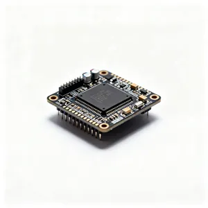
3D integrated circuits have changed electronics by stacking layers. Engineers can fit more circuits into a small space. HiSilicon uses this stacking in chips for phones and wearables. They stack layers on top of each other. This makes the chips smaller and more powerful. It helps make small devices that still work well.
Stacking layers does more than save space. Shorter connections between layers use less power. This makes data move faster. Devices can work at higher speeds. The table below shows how stacking helps circuits in different ways:
|
Benefit Area |
Technical Support and Application Examples |
|---|---|
|
Performance Improvement |
Shorter connections mean less delay and less power use. Data moves faster and devices work better. |
|
Space Efficiency |
Stacking puts more parts in a small area. This is good for phones and wearables. |
|
High-Performance Computing |
Stacking memory and processors makes data move faster. It also lowers wait times in big computers. |
|
Power and Thermal Management |
Power spreads out better and heat moves away faster. This keeps devices safe and working longer. |
|
Design Flexibility |
Parts can be placed in better spots. This helps signals stay strong and saves power. |
Stacking also helps store more energy and filter signals better. Engineers see smoother voltage and less signal loss. These changes help make electronics smaller, smarter, and more reliable.
Heterogeneous Integration
Heterogeneous integration puts different chips together in one package. HiSilicon uses this for smart chips, controllers, and optical parts. This helps with AI, IoT, and smart media. By using this method, engineers make systems work better and add more features.
-
Vertical stacking lets more connections fit in a small space. This saves power and helps signals move better.
-
Die-to-wafer bonding makes tiny connections. This lets more parts fit together.
-
3D technology makes thin, light chips with many parts. This helps the whole system work better.
Putting different chiplets together has many benefits:
-
Shorter wires make signals move faster and reduce delays.
-
Putting parts together saves space and uses less power.
-
It costs less because building is easier and more chips work right.
-
It lets engineers make special designs for many uses.
-
Chips are easier to fix and last longer.
This way of making circuits helps make things smaller and smarter. It also lets engineers create new and better electronics for many uses.
Development of 3D Integrated Circuits
Key Innovations
The growth of 3D integrated circuits has brought many big changes. Early integrated circuits were simple. Now, engineers use vertical stacking, 3D-MID, and new materials like gallium nitride and carbon nanotubes. These updates help make devices smaller, faster, and more reliable. The table below shows how new ideas have changed things over time:
|
Year/Period |
Key Innovation/Event |
Numerical Data / Details |
|---|---|---|
|
1947 |
Invention of the transistor |
N/A |
|
1952 |
Conceptual proposal of integrated circuits |
N/A |
|
1958 |
First working IC prototype by Jack Kilby |
Prototype used germanium and hand-connected gold wires |
|
1959 |
Silicon planar IC by Robert Noyce |
Enabled mass production via photolithography |
|
1971 |
Intel 4004 microprocessor |
2,300 transistors |
|
1980s-1990s |
Very Large-Scale Integration (VLSI) |
Chips with millions of transistors |
|
Early 2000s |
Node size ~90nm |
Start of FinFETs |
|
22nm node |
FinFET transistor architecture |
3D transistor structure improves performance |
|
3nm and below |
Gate-All-Around FETs (GAAFETs) |
Enhanced control and efficiency |
|
Present |
3D integration technologies (TSVs, chiplets, fan-out) |
Enables vertical stacking and modular chip architectures |
|
Present |
Packaging innovations (chiplets, fan-out wafer-level) |
Boosts performance and reduces power consumption |
Engineers use wafer-to-wafer and die-to-wafer bonding to line up parts better and make them stronger. These ways let them stack layers on top of each other. This saves space and makes things work faster. For example, high-bandwidth memory in NVIDIA GPUs can reach 1.5 TB/s. AMD’s 3D V-Cache gives a 15% speed boost. Apple’s A-series chips use stacked memory for faster speeds and better power use. These examples show how new ideas help make smart devices and automation better.
Industry Impact
3D integrated circuits have changed many industries. Companies use them in electronics, cars, planes, and medical tools. These areas need smaller, faster, and more energy-saving circuits. For example, Mobileye’s EyeQ5 chip can handle data from eight cameras at once. This helps with advanced driver assistance. Infineon’s HybridPACK™ Drive makes electric cars more powerful by 40%. In medical tools, 3D integrated circuits help make equipment smaller and smarter for patients.
The global market for 3D integrated circuits is growing quickly. Reports say it could reach $92.72 billion by 2032, with a CAGR of 33%. This growth comes from the need for fast computing, AI, and automation. Big companies like Intel, Samsung, and TSMC are investing in chiplet ecosystems and new packaging. These new technologies help save energy and cut down on waste.
Car, plane, and healthcare companies get better performance, more bandwidth, and smaller circuits. New ideas and more automation keep pushing the use of 3D integrated circuits in these fields.
Miniaturization and Performance
Space Savings
3D integrated circuits help make devices much smaller. Engineers stack layers of circuits on top of each other. This saves space compared to flat designs. Devices like smartphones and wearables can be thinner and lighter. The CHIP approach uses both sides of a chip for circuits. This makes the design compact and adds more connections in a small area.
Researchers have measured how much smaller devices can get. Devices with 3D integrated circuits can be up to 1,000 times smaller than regular chips. Engineers also use six times more wafer area with 3D interconnects. These changes let more circuits fit in the same space. Devices can do more things without getting bigger. The table below shows some of these improvements:
|
Metric / Improvement |
Description |
|---|---|
|
Device area reduction |
3 orders of magnitude smaller device area compared to standard chips |
|
Wafer area utilization |
6-fold increase in wafer area use enabled by 3D interconnects |
|
Fabrication techniques |
Advanced methods like plasma etching and gold electrodeposition |
|
Wafer bonding |
Handling of ultra-thin films for stacking |
|
Additional benefits |
Small shading factor below 3%, enabling high-density and miniaturized photonic power devices |
These advances help make smaller electronic devices. Phones, tablets, and smartwatches now have more features in less space. Engineers can add sensors and other parts without making devices bigger. This helps meet the need for smaller and smarter products.
Note: Miniaturization saves space and lets engineers make new shapes. They can build flexible devices that bend and twist without breaking.
Energy Efficiency
3D integrated circuits help devices use less energy. Engineers at The University of Tokyo made new nanosheet oxide semiconductors. These materials help circuits work better and waste less power. The process uses low temperatures, which stops charge from leaking and supports high voltages. Devices become more reliable and use less energy.
Monolithic 3D ICs stack layers closely and use tiny connections. This makes signals travel shorter distances. It lowers energy use and speeds up data movement. Engineers also put different types of memory and logic together in one stack. This cuts down on energy needed for data transfer and makes devices work better.
-
Monolithic 3D ICs make devices more energy efficient.
-
Stacking memory and logic lowers latency and energy use.
-
Hybrid memory, like SRAM and MRAM, saves energy and keeps performance high.
-
Stacked multiply-accumulate units with close connections use less energy and keep chips cooler.
-
Better thermal management helps 3D ICs run cooler and more efficiently.
The table below shows some key ways 3D integrated circuits save energy:
|
Metric |
Description |
|---|---|
|
Latency |
Time delay in data transmission within the 3D network-on-chip (NoC) architecture. |
|
Energy-Delay-Product |
Combines network latency and energy use to measure overall efficiency. |
Consumer electronics last longer on one charge and make less heat. Through-Silicon-Vias (TSVs) and hybrid bonding also help move data faster between layers. These changes help make smaller devices that can do more things.
Advanced Packaging
Connectivity Improvements
Advanced packaging helps parts inside circuits connect better. Engineers use wafer-level packaging to line up parts very carefully. This makes strong and fast connections. High-bandwidth memory uses these fast links to move data quickly and save energy.
-
Wafer-level packaging lines up parts well and makes fast links. High-bandwidth memory needs these fast and low-energy connections.
-
Heterogeneous integration puts CPUs, GPUs, memory, and I/O dies together. This packs more links in a small space and makes signals clearer.
-
3D integrated circuits and chiplet designs put dies close together. This helps data move faster and saves energy.
-
These new ways let parts talk faster and better inside one package.
-
Automation and careful testing help make sure connections work well and most chips are good.
Tests show advanced packaging keeps signals strong and cuts down on delays. Engineers use atomic force microscopy and white light interferometry to check tiny alignments. AI inspection finds problems fast and keeps quality high. Hybrid bonding makes very tiny links, just a few microns wide. Some packages now move over 1000 GB of data each second.
Thermal Management
Thermal management is important for circuits. New packaging spreads heat and keeps things cool. Engineers tried flat heat spreaders and vapor chambers to lower heat. These tools make devices safer and more reliable.
|
Feature/Innovation |
Details/Outcome |
|---|---|
|
Boiling-driven two-phase flat heat spreader |
Lowered temperature difference to 7.6 °C at 1500 W. This is better than 28 °C with copper. Thermal resistance is less than 0.2 K/W. |
|
Bubbles escape well in any position. Lowest thermal resistance is 0.17 K/W at 200 W/cm². |
|
|
Deep learning models guess chip temperatures right away. This helps cool high-density circuits. |
These new packaging ideas help circuits handle more power and stay safe. Better thermal management lets devices run faster and last longer. This helps make electronics smaller and smarter for many jobs.
Future of 3D
Ongoing Research
Researchers keep working to make integrated circuits better. They want devices to be smaller, faster, and more reliable. Some studies look at Through-Silicon Vias and monolithic 3D integrated circuits. Monolithic 3D designs can have up to 10,000 times more vertical connections than older ways. This means devices can work much better and be smaller. But these new designs also bring some problems. Heat can build up fast in stacked layers. It also costs a lot to design these circuits. Scientists are trying things like special insulators that move heat away and very thin transistors. These ideas help control heat and make devices last longer.
A new 3D X-ray imaging tool lets engineers see inside circuits at 4nm resolution. This helps them check if chips are made well without breaking them. It also helps them find and fix problems faster. These new tools make it easier to build 3D circuits that work well and are made right.
Trends and Challenges
The future for 3D circuits looks bright with lots of chances to grow. There are some big trends in this area:
-
The global market for integrated circuits is growing quickly. Experts think it will be over $40 billion by 2032.
-
Making things smaller is still very important. More areas like electronics, healthcare, and cars need tiny, smart devices.
-
New ways to make and design circuits help them do more and use less energy.
-
Automation, AI, IoT, and 5G make people want even better circuits.
-
Companies spend money on new ideas to make technology better and cheaper.
But there are still some problems to solve:
|
Challenge |
Impact |
|---|---|
|
High power makes heat problems in stacked layers. |
|
|
Manufacturing cost |
New packaging and design make things cost more. |
|
Yield and reliability |
Mistakes and hard assembly lower how many good chips are made. |
|
Scalability |
Making circuits smaller and more complex is hard and costs more. |
The future of 3D circuits depends on fixing these problems. New ideas and more automation will help make circuits smaller and better.
3D integrated circuits are starting a new time in electronics. These circuits help make devices smaller and smarter. They also make electronics work faster and send data quicker. Many companies use these circuits to add more features in less space. The table below shows how the market is growing. More companies want better and smaller electronics for people to use.
|
Statistic/Segment |
Value (2024) |
Projected Value (2034) |
CAGR (%) |
Significance |
|---|---|---|---|---|
|
Global 3D IC Market Size |
US$ 22.1 billion |
US$ 129.12 billion |
19.3 |
Rapid adoption due to miniaturization and enhanced performance |
|
3D Wafer-Level Chip-Scale Packaging (WLCSP) Segment |
US$ 11.96 billion |
US$ 67.66 billion |
18.4 |
Downsizing and performance benefits |
|
Japan Market CAGR |
N/A |
N/A |
20.5 |
Strong regional growth driven by 3D IC technology |
|
East Asia Market Share (2024) |
32.5% |
N/A |
N/A |
Dominant regional market share for smaller, powerful devices |
3D integrated circuits will keep changing how people use technology. These new circuits will help improve communication, healthcare, and everyday life.
FAQ
What makes 3D integrated circuits different from regular chips?
3D integrated circuits have layers stacked on top of each other. Regular chips only have one layer. Stacking layers saves space. It also helps devices work faster.
How do 3D ICs help save energy?
3D ICs have short connections between layers. Signals do not travel far. This design uses less power. Devices also make less heat.
Where can people find 3D integrated circuits in daily life?
People use 3D ICs in smartphones and smartwatches. They are also in medical devices. You can find them in computers and cars too.
What challenges do engineers face with 3D ICs?
Engineers need to fix heat and cost problems. Stacked layers get hot fast. Making these chips costs a lot of money.
Are 3D integrated circuits safe for the environment?
Many 3D ICs use less energy and space. This helps cut down on electronic waste. Companies are working to make production safer for the planet.