Analog Design in Action: A Case Study of a Sensor Interface Circuit from Concept to Prototype
Expert guide on Analog Design in Action: A Case Study of a Sensor Interface Circuit from Concept to Prototype. Technical specs, applications, sourcing tips for engineers and buyers.
Analog Design in Action: A Case Study of a Sensor Interface Circuit from Concept to Prototype
Every seasoned analog engineer has a story about a sensor interface that looked perfect on the bench but fell apart in the field. A pressure transmitter that drifted with temperature, a strain gauge that picked up motor noise, or a ratiometric design that lost accuracy because someone swapped the reference. These failures aren’t academic—they cost PCB spins, delayed shipments, and eroded trust. In this case study, we’ll walk through a real-world sensor interface design from concept to prototype, exposing the decisions that separate a robust product from a support nightmare. Along the way, we’ll tackle the common ratiometric design dilemma that trips up even experienced designers and apply the EE Times guide to ADC interface challenges to keep the signal chain honest.
Why Sensor Interface Design Still Trips Up Engineers
On paper, connecting a sensor to an ADC looks trivial: excite the sensor, buffer the signal, maybe add a filter, and digitize. In practice, the analog front-end is where most IoT and industrial products earn their reliability—or lose it. The case we’ll follow involves a 350 Ω strain-gauge pressure sensor that must deliver 0.1% accuracy over -20°C to +85°C, with a BOM cost target under $3.50 for the entire signal chain. The design team initially chose a simple non-inverting amplifier and a 12-bit SAR ADC with an internal reference. The first prototype failed miserably: output noise was 10× higher than expected, and the reading drifted by 2% when the 3.3 V rail sagged under load.
Why? Because the sensor excitation and ADC reference came from different voltage sources. The ratiometric advantage was lost. As the StackExchange discussion on analog sensor design highlights, many engineers underestimate how supply variations couple into the measurement when the bridge and ADC reference aren’t tied together. The EE Times article on sensor-to-ADC interfaces reinforces this: the ADC must have enough effective bits to resolve the sensor’s smallest meaningful change, but resolution without ratiometric tracking is wasted. These pain points—noise, reference drift, and layout-induced errors—are what we’ll solve step by step.
From Sensor to ADC: The Signal Chain Fundamentals
Before choosing components, you need to map the signal chain blocks and their critical parameters. For our pressure sensor, the chain consists of excitation, the bridge sensor itself, differential amplification, anti-aliasing filtering, and the ADC. The table below captures the key design parameters we derived from the sensor datasheet and system requirements.
| Parameter | Value/Range | Unit/Notes |
|---|---|---|
| Sensor type | 350 Ω strain gauge bridge (4-wire) | Full bridge, 2 mV/V sensitivity |
| Excitation voltage (VEXC) | 3.3 V (ratiometric with ADC reference) | Same supply as ADC VREF |
| Full-scale output (FSO) | ±6.6 mV (differential) | At rated pressure, VEXC × sensitivity |
| Required resolution | 0.1% of FSO | ~6.6 µV per LSB |
| ADC resolution (minimum) | 16 bits (effective) | After accounting for noise; 12-bit insufficient |
| Input range (ADC) | ±VREF/gain | PGA gain = 128, VREF = 3.3 V → ±25.8 mV |
| Sampling rate | 100 SPS | Sufficient for pressure monitoring |
| Anti-aliasing filter cutoff | 10 Hz | Single-pole RC, placed after amplifier |
| Amplifier gain | 128 V/V | Instrumentation amplifier, low drift |
| Noise target (input-referred) | < 1 µVRMS (0.1–10 Hz) | To preserve 0.1% accuracy |
| Operating temperature | -20°C to +85°C | Industrial range |
These numbers aren’t arbitrary. The ratiometric approach—using the same 3.3 V rail for both bridge excitation and ADC reference—cancels supply drift, as detailed in the Analog Devices low-cost sensor interface article. The article demonstrates how powering multiple sensors in parallel from the same reference supply eliminates reference errors, a technique we adopted. For the amplifier, we selected an instrumentation amplifier with a gain of 128 to map the tiny ±6.6 mV differential signal to nearly the full ADC input range. The practical signal conditioning handbook and its companion PDF provide detailed bridge circuit topologies and AC excitation techniques that can eliminate offset drift, though for our cost-sensitive design we stayed with DC excitation and chopper-stabilized amplifiers.
Noise bandwidth is the silent killer. The MS-2066 technical article shows that narrowing the bandwidth with a simple RC filter after the sensor can slash output noise from millivolts to microvolts. In our prototype, a 1.6 kΩ resistor and 10 µF capacitor created a 10 Hz low-pass filter that reduced wideband noise by a factor of 20, without expensive components. The key is placing the filter after the amplifier, where the signal is larger and less susceptible to resistor thermal noise.
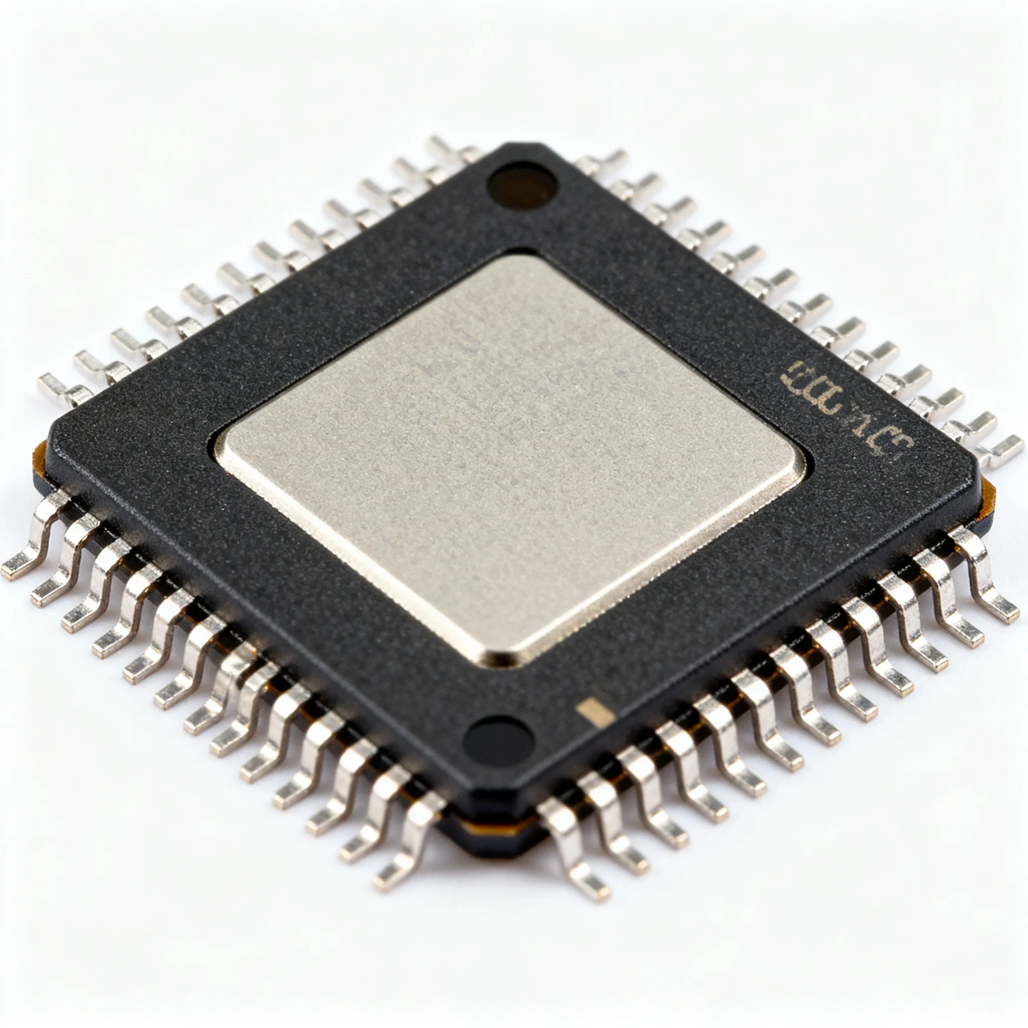
Choosing the Right ADC and Front-End Architecture
With the signal chain parameters defined, the next fork in the road is architecture: discrete amplifier plus standalone ADC, an integrated analog front-end (AFE) with built-in PGA and ADC, or a fully integrated sensor module. Each path has trade-offs in cost, flexibility, and supply chain complexity. The table below compares three representative solutions that fit our pressure sensor case.
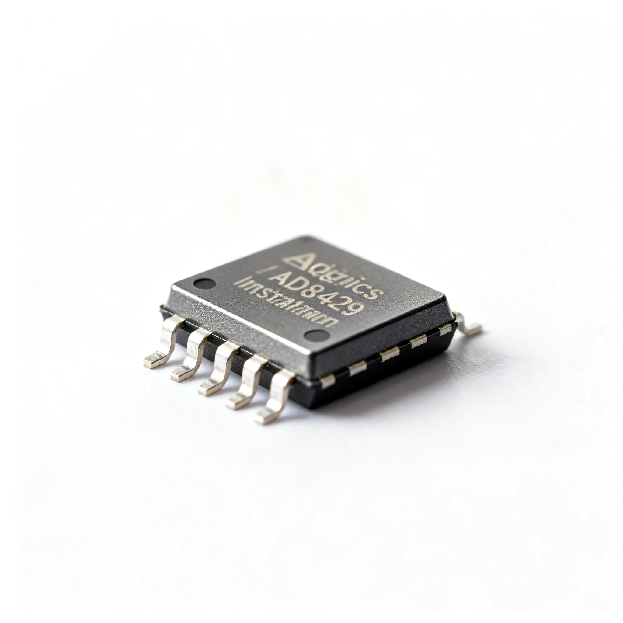
| Comparison Metric | Option A: Discrete In-Amp + SAR ADC (AD8226 + AD7091R) | Option B: Integrated AFE (AD7124-8) | Option C: Fully Integrated Sensor Module (ADIS16240) | Selection Criteria & Failure Boundary |
|---|---|---|---|---|
| Component count | 2 ICs + passives | 1 IC + minimal passives | 1 module (sensor + signal chain) | Higher count increases PCB area and assembly cost; Option C eliminates external sensor sourcing. |
| BOM cost (1k qty) | ~$2.80 | ~$4.50 | ~$25.00 | Option A meets tight cost targets; Option C justified only when sensor integration adds value. |
| Noise performance (input-referred) | 0.8 µVRMS (with external filter) | 0.5 µVRMS (internal PGA + digital filter) | 1.5 µVRMS (sensor noise dominates) | Option B offers best noise for high-resolution needs; Option A adequate for 0.1% accuracy. |
| Ratiometric capability | Yes, if VREF tied to VEXC | Yes, internal reference can be bypassed | Internal regulated excitation; not ratiometric | Ratiometric design cancels supply drift; Option C uses internal LDO, so supply rejection must be verified. |
| Supply chain risk | Multi-source amplifiers and ADCs | Single-source AFE (ADI) | Single-source module (ADI) | Option A reduces single-source dependency; Option B/C require buffer stock or second-source qualification. |
| Flexibility | High—choose gain, filter, ADC separately | Moderate—configurable PGA, filter, and ADC modes | Low—fixed sensor type and range | Option A best for custom sensors; Option C quickest to prototype but locks sensor choice. |
The EE Times selection criteria emphasize that the ADC must have enough bits to resolve the required accuracy, but also that the interface structure (single-ended vs. differential, ratiometric vs. absolute) determines real-world performance. The MAX1238 example from Analog Devices illustrates a 12-input multiplexed ratiometric system where the positive supply serves as both excitation and reference—a clever trick for multi-sensor arrays. For our single pressure sensor, we chose Option A (discrete in-amp + SAR ADC) because it hit the cost target and allowed us to fine-tune the filter. However, we kept the ADIS16240 integrated impact sensor in mind as a fallback: its fully integrated signal chain and digital output would have slashed development time if the discrete path ran into trouble. The ADIS16240 datasheet shows how a module can simplify procurement by collapsing multiple line items into one, but at a premium.
Tip: When comparing architectures, always simulate the noise budget with real component values. A 16-bit ADC doesn’t guarantee 16 noise-free bits; the effective resolution is limited by the amplifier’s input noise and the reference’s drift. In our case, the AD7091R’s 12-bit core was insufficient, so we moved to a 16-bit SAR ADC with a lower noise floor, proving that resolution specs must be validated against the sensor’s full-scale output.
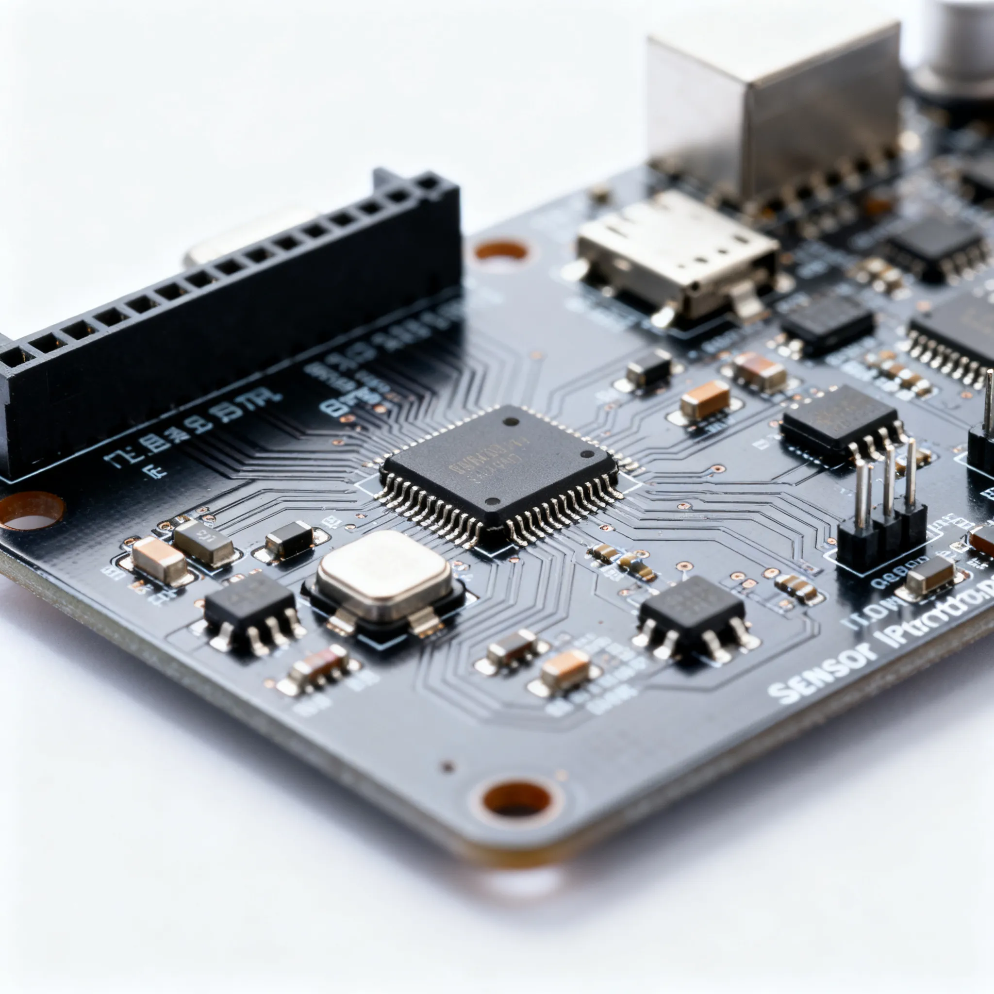
Prototyping Pitfalls and Procurement Insights
Moving from schematic to prototype is where theory meets copper. Our first board revision suffered from 50 Hz hum that swamped the pressure signal. The root cause? A ground loop formed because the sensor cable shield was grounded at both ends. The fix—a single-point ground at the ADC—cost a PCB spin but taught a valuable lesson. The table below captures the most common prototyping pitfalls we encountered and the procurement strategies that kept the project on track.
| Pitfall | Symptom | Root Cause | Mitigation Strategy | Procurement Impact |
|---|---|---|---|---|
| Ground loops | 50/60 Hz periodic noise on ADC readings | Multiple return paths; shield grounded at both ends | Single-point grounding; break shield at sensor end | No extra BOM cost, but layout revision may delay prototypes. |
| Ratiometric error | Output drifts with supply voltage changes | ADC reference and sensor excitation from different rails | Tie VREF and VEXC to same supply; use ratiometric ADC | May require ADC with external reference input; check availability. |
| ADC input overdrive | Clipped readings or latch-up | Amplifier output exceeds ADC input range during startup or fault | Add series resistor and Schottky clamps to ADC inputs | Adds pennies to BOM; ensure clamping diodes are in stock. |
| Long lead times on precision resistors | Prototype build delayed by 8–12 weeks | 0.1% thin-film resistors in non-standard values allocated | Design with standard E96 values; qualify second-source thick-film arrays | Work with distributors like IC-Online to find in-stock alternatives with flexible MOQs. |
| Inadequate filtering | Noisy readings despite low-noise amplifier | Bandwidth too wide; no anti-aliasing before ADC | Add passive RC filter with cutoff ≤ 1/10 sampling rate | Resistors and capacitors are commodity; no lead-time risk. |
| Single-source ADC allocation | Production halted when ADC went out of stock | Proprietary ADC with no pin-compatible alternative | Select ADCs with multiple sources or pin-compatible families; pre-negotiate buffer stock | Use TechInsights’ competitive pricing analysis to benchmark costs and identify second sources early. |
The TechInsights case study on analog IC pricing underscores how competitive benchmarking can prevent overpaying for single-sourced parts. In our project, we discovered that a pin-compatible ADC from a second manufacturer was 18% cheaper and had shorter lead times, simply by cross-referencing the market before freezing the BOM. The StackExchange ratiometric ADC discussion also reminded us that ratiometric designs can reduce dependency on expensive precision voltage references—another procurement win. By using the same 3.3 V rail for excitation and reference, we eliminated a $0.75 reference IC and its associated passives.
Filtering is your cheapest insurance. The MS-2066 filtering guidance shows that a well-chosen RC filter can improve SNR by 30 dB without adding active circuitry. We applied a 10 Hz single-pole filter right at the ADC input, using a 1.6 kΩ resistor and a 10 µF ceramic capacitor. The total cost: $0.04. The improvement in noise floor: from 120 µVRMS to 4 µVRMS. That’s the kind of value that keeps both engineers and procurement managers happy.
Sensor Interface FAQs for Engineers and Buyers
Q: When should I use a ratiometric ADC instead of a precision voltage reference?
A: Use a ratiometric ADC when the sensor excitation and ADC reference can share the same supply, eliminating reference drift errors. This is ideal for resistive bridges and many low-cost sensors, as detailed in the Analog Devices low-cost interface article. If the sensor output is proportional to its supply voltage, a ratiometric connection cancels out supply variations, making a precision reference unnecessary. However, if the sensor requires an absolute voltage reference (e.g., thermocouple with cold-junction compensation), a ratiometric approach won’t work.
Q: How do I select the right ADC resolution for my sensor?
A: Match the ADC’s effective number of bits (ENOB) to the sensor’s dynamic range and required accuracy. A common pitfall is over-specifying resolution without accounting for noise; a 24-bit ADC may deliver only 16 noise-free bits in a real circuit. The EE Times interface guide explains how to balance resolution, speed, and power. For our pressure sensor with 0.1% accuracy, a 16-bit ADC with an ENOB of 14.5 bits was sufficient after filtering. Always calculate the LSB size relative to the sensor’s smallest expected signal change.
Q: What are the hidden costs in sensor interface prototyping?
A: Beyond the BOM, hidden costs include multiple PCB spins due to noise or layout issues, extended test time for calibration, and procurement delays for precision passives. The TechInsights case study shows how competitive pricing analysis can prevent overpaying for analog ICs. In our project, one extra PCB spin cost $2,500 and two weeks of schedule, all because of a ground loop that could have been avoided with a design review. Factor in calibration fixtures and temperature chamber time as well.
Q: How can I mitigate noise without increasing BOM cost?
A: Use passive RC filtering after the sensor, choose amplifiers with appropriate bandwidth, and leverage the ADC’s internal digital filtering. MS-2066 demonstrates that narrowing bandwidth with the right RC values dramatically improves SNR without expensive components. In our design, a $0.04 RC filter reduced noise by a factor of 30. Also, keep high-impedance nodes small and guard them from digital traces—layout is free.
Q: What procurement risks should I watch for with analog ICs?
A: Watch for single-source ADCs or specialty amplifiers with long lead times. The ADIS16240 data sheet illustrates a fully integrated alternative that can simplify the supply chain by replacing multiple line items with one module. However, that module itself may be single-source. The StackExchange discussion highlights how ratiometric designs can reduce dependency on precision voltage references, which are often allocated. Always qualify a second-source ADC or negotiate buffer stock agreements with distributors like IC-Online.
Q: How do I validate a sensor interface prototype before committing to production?
A: Perform noise floor measurements, test with worst-case sensor tolerances, and verify performance over temperature. The practical design techniques from Analog Devices’ signal conditioning handbook provide a step-by-step validation approach that catches issues early. We ran a 24-hour drift test at 85°C, injected known pressure steps, and measured the ADC output histogram to confirm noise distribution. Only after passing these tests did we release the BOM for production.
References & Further Reading
- How to properly design a circuit for an analog sensor? – Electrical Engineering Stack Exchange
- Improving Sensor to ADC Analog Interface Design...Part One – EE Times
- Design Considerations for a Low-Cost Sensor and A/D Interface – Analog Devices
- Analog Devices – Practical Design Techniques For Sensor Signal Conditioning (Scribd)
- Practical Design Techniques for Sensor Signal Conditioning (PDF)
- Technical Article MS-2066: Noise Reduction in Sensor Signal Chains – Analog Devices
- ADIS16240 Low Power, Programmable Impact Sensor and Recorder Data Sheet – Analog Devices
- Analog Device Analysis and Competitive Pricing – TechInsights
- IC-Online – Electronic Components Sourcing and Procurement
For mixed BOM requirements and flexible MOQs on analog ICs, visit IC-Online to compare inventory and pricing from multiple authorized distributors.