PCB Manufacturing and Assembly: From Design to Finished Product
You start with a design and watch it become a working circuit board. Each step in PCB Manufacturing matters, from the first drawing to the final test. The industry keeps growing fast. For example, the global PCB market could reach $120 billion by 2030. AI helps you finish designs up to 70% faster and reduces mistakes.
You start with a design and watch it become a working circuit board. Each step in PCB Manufacturing matters, from the first drawing to the final test. The industry keeps growing fast. For example, the global PCB market could reach $120 billion by 2030. AI helps you finish designs up to 70% faster and reduces mistakes.
New factories and better machines help you get high-quality boards quickly. If you follow best practices, you build reliable products for any use.
Key Takeaways
-
Start your PCB project with careful design, using tools like schematic audits and simulations to catch errors early and save time and money.
-
Choose the right materials and follow precise manufacturing steps like imaging, drilling, and plating to build strong, reliable circuit boards.
-
Use automated assembly methods like SMT for speed and accuracy, and apply thorough cleaning and protective coatings to ensure long-lasting performance.
-
Perform detailed testing with AOI, in-circuit, and functional tests to find defects early and guarantee your boards work as intended.
-
Protect your finished PCBs with proper packaging and choose reliable shipping methods to avoid damage and ensure timely delivery.
Design
Schematic
You begin the PCB journey with the schematic. This is your blueprint. You draw the electrical connections and place each component. During this phase, you run a Schematic Audit Report. This report checks for errors in connectivity, device selection, and electrical rules. You also use circuit simulation to test how your design works before moving forward. Power analysis helps you confirm that each chip gets the right voltage and current. Early detection of mistakes here saves you time and money later.
Layout
Next, you move to the layout. You arrange the components on the board and route the traces. You must follow spacing rules to prevent shorts and signal problems. Good layout helps your board work reliably and makes assembly easier. You use design software to check for errors as you go. This step shapes how your board will look and perform.
DFM and DFA
Design for Manufacturability (DFM) and Design for Assembly (DFA) are key principles. You make choices that help the board get made and assembled without trouble. About 70-80% of production costs come from decisions you make during design. Early choices affect your budget, materials, and how fast you can launch your product. Good communication with your team at this stage reduces redesigns and speeds up your project.
-
The PCB market has grown to over $60 billion since 2012, showing how important careful design is.
-
Early design decisions shape cost, materials, and time to market.
Prototyping
You build a prototype to test your design in the real world. This step lets you catch problems before full production. You can make changes quickly and avoid expensive mistakes.
File Output
You finish by preparing files for manufacturing. You run a Design Rule Check (DRC) to catch layout errors. You preview each layer to check for missing or misaligned parts. CAM verification simulates the manufacturing process to spot issues early.
|
Aspect |
Description |
Importance/Benchmark |
|---|---|---|
|
Industry design and quality rules |
Ensures reliability and manufacturability |
|
|
Correct hole sizes and placements |
Prevents mechanical and electrical failures |
|
|
DFM Review Process |
File checks before Gerber generation |
Reduces errors and aligns with manufacturer needs |
Tip: Always double-check your files and follow your manufacturer’s guidelines to avoid delays and extra costs.
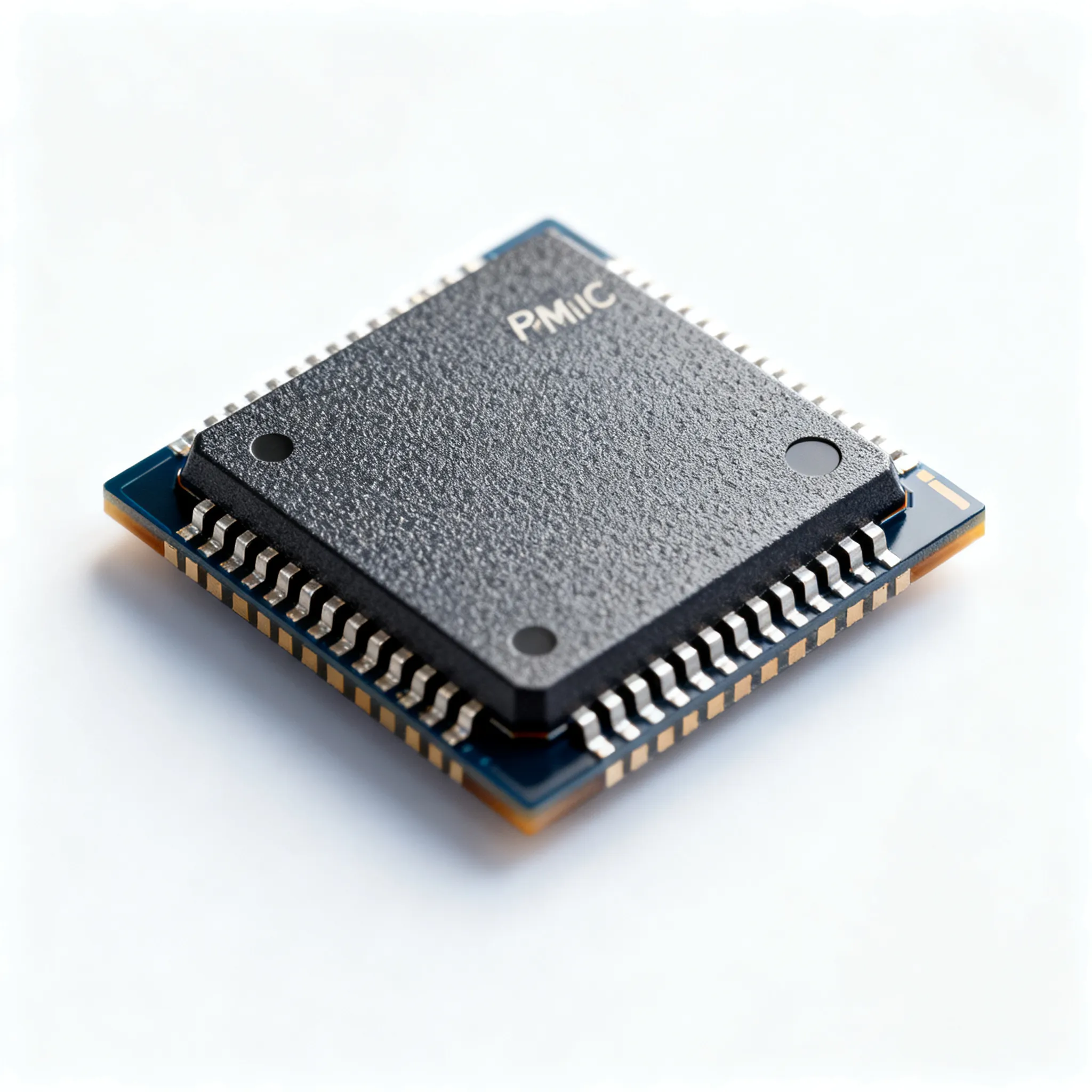
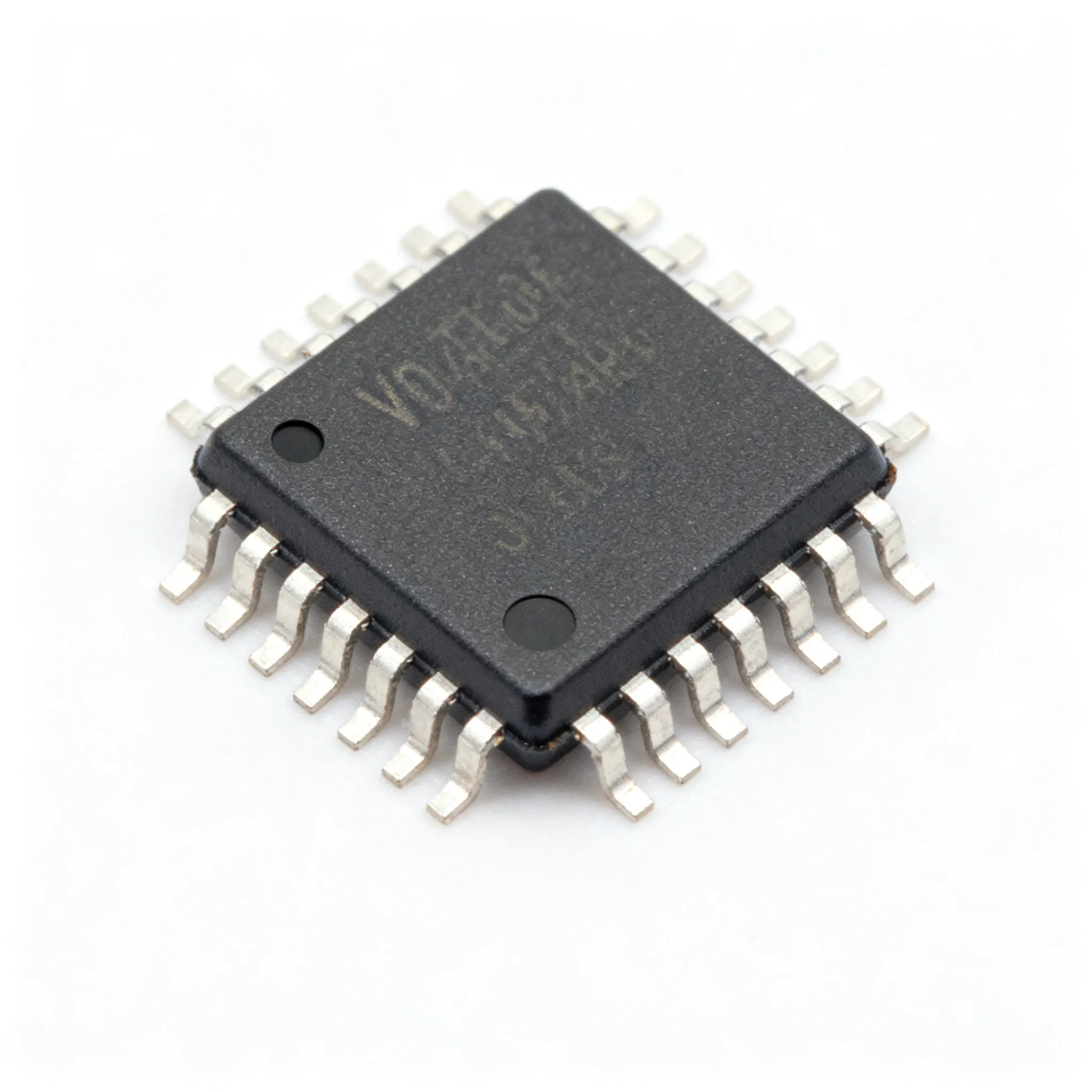
PCB Manufacturing
Material Selection
You start PCB Manufacturing by choosing the right materials. Your choice affects how strong, reliable, and cost-effective your board will be. FR4 is the most common material. It works well for most electronics. If you need better heat resistance or lower moisture absorption, you might pick CF 004. The table below shows how these materials compare:
|
Performance Indicator |
FR4 |
CF 004 |
|---|---|---|
|
Dielectric Constant (Dk) |
4.4 – 4.6 |
3.8 – 4.2 |
|
Thermal Conductivity (W/m·K) |
0.25 – 0.35 |
0.35 – 0.45 |
|
Glass Transition Temperature |
130 – 180°C |
150 – 200°C |
|
Moisture Absorption |
<0.15% |
<0.1% |
|
Cost |
Moderate |
Moderate to High |
|
Typical Applications |
Consumer electronics |
Aerospace, defense |
You should always match your material to your project’s needs.
Imaging and Etching
Next, you transfer your design onto the board. You use a photoresist layer and shine light through a mask. This step creates the pattern for your copper traces. Then, you remove unwanted copper using a chemical etching process. This leaves only the paths you need for your circuit.
Layer Alignment
If your board has more than one layer, you must align them carefully. You use special markers and machines to stack the layers with high precision. Even a small misalignment can cause your board to fail. Good alignment keeps your signals clear and your board reliable.
|
Measurement Type |
Impact on PCB Performance |
|
|---|---|---|
|
Drilled Holes Diameter |
±0.05 mm |
Ensures proper alignment and electrical connectivity |
|
Trace Width and Spacing |
±0.05 mm to ±0.1 mm |
Maintains signal integrity and prevents short circuits |
|
Board Dimensions |
±0.1 mm to ±0.2 mm |
Ensures fit within enclosures |
Drilling and Plating
You drill holes for component leads and connections between layers. Machines keep hole size and shape very accurate. Clean, round holes help the next step—plating. You coat the inside of each hole with copper. This connects the layers and makes your board strong.
Solder Mask and Silkscreen
You cover your board with a solder mask. This green (or sometimes other color) layer protects the copper and keeps solder only where you want it. You add silkscreen markings to show part numbers, logos, or other helpful info.
Surface Finish
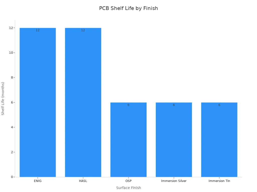
You add a surface finish to protect the copper and help with soldering. ENIG (Electroless Nickel Immersion Gold) is a popular choice for high-reliability boards. It gives a flat, long-lasting surface. Other finishes like HASL and OSP are cheaper but may not last as long. The right finish helps your board survive storage and assembly.
AOI and Inspection
You use Automated Optical Inspection (AOI) to check for defects. AOI systems find problems with up to 99% accuracy, much better than manual checks. This step helps you catch mistakes early and keeps your PCB Manufacturing process reliable. Companies like NOVA PBCA, working since 2007, use AOI and strict inspections to deliver high-quality boards every time.
Tip: Careful inspection at every stage helps you avoid costly rework and ensures your finished product meets industry standards.
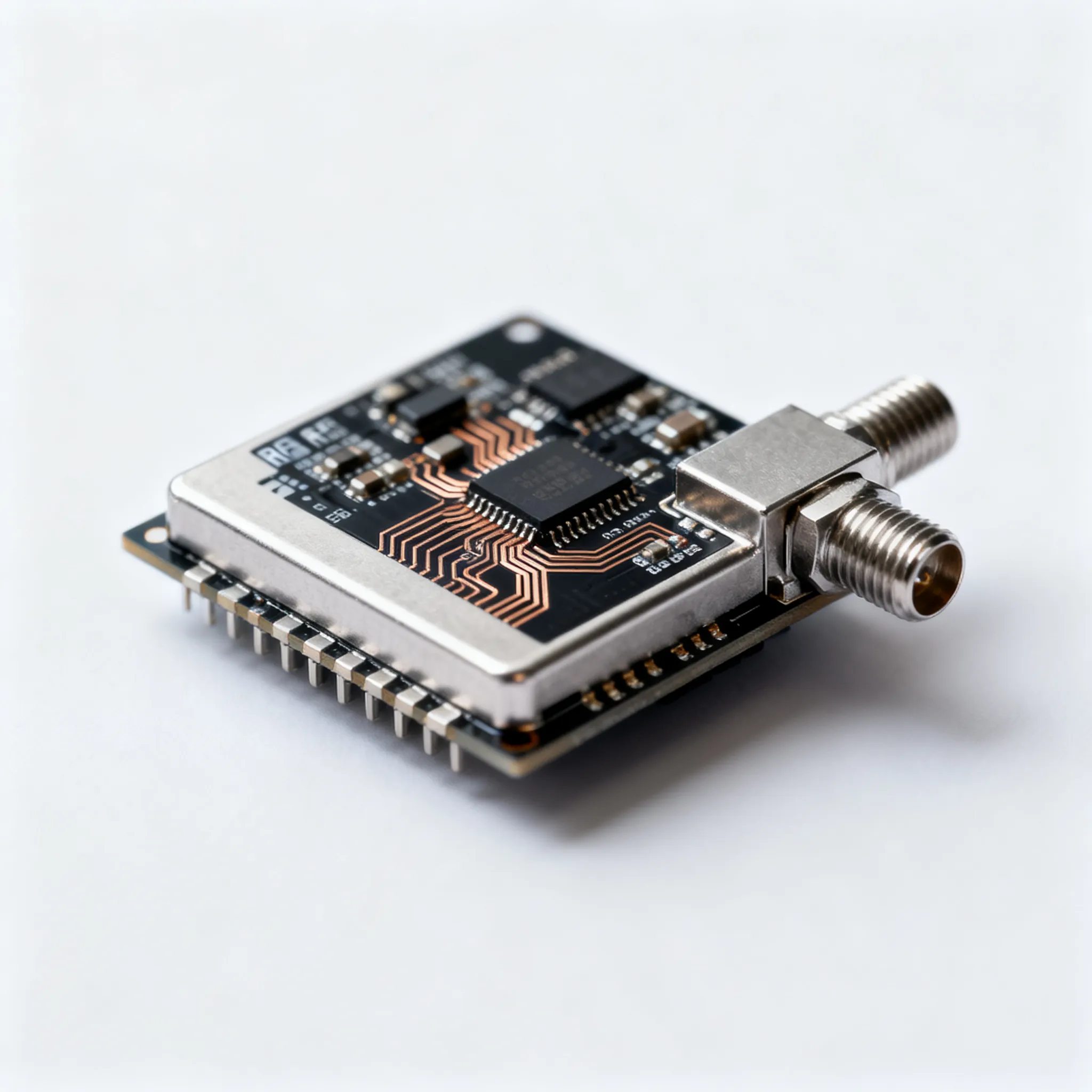
Assembly
Component Sourcing
You start assembly by finding the right parts for your board. Good sourcing keeps your project on schedule and within budget. You check each supplier for quality, delivery speed, and support. Automation tools help you track supplier performance in real time. This lets you spot delays or problems before they affect your build.
|
Metric / Criterion |
Description / Impact |
Validation Role in Sourcing Strategy |
|---|---|---|
|
Metrics to assess sourcing efficiency |
Track sourcing efficiency and identify improvement areas |
|
|
Bottleneck Identification |
Regular performance reviews to spot slowdowns |
Detect delays or issues affecting component availability |
|
Delivery Performance History |
On-time delivery rates and delivery speed |
Ensure suppliers meet production schedules |
|
Supplier Responsiveness |
Engagement and communication speed |
Facilitate proactive issue resolution and maintain smooth workflow |
|
Quality Control Processes |
Inspections, testing, and certifications |
Minimize defects and ensure component quality |
|
Inventory Management Metrics |
Lead times, reorder points, and inventory levels |
Balance stock to avoid shortages or excess, supporting JIT practices |
|
Customer Support Availability |
Support team responsiveness and availability |
Provide assistance to resolve sourcing or quality issues |
Tip: Always review supplier history and quality checks before placing large orders. This helps you avoid shortages and defects.
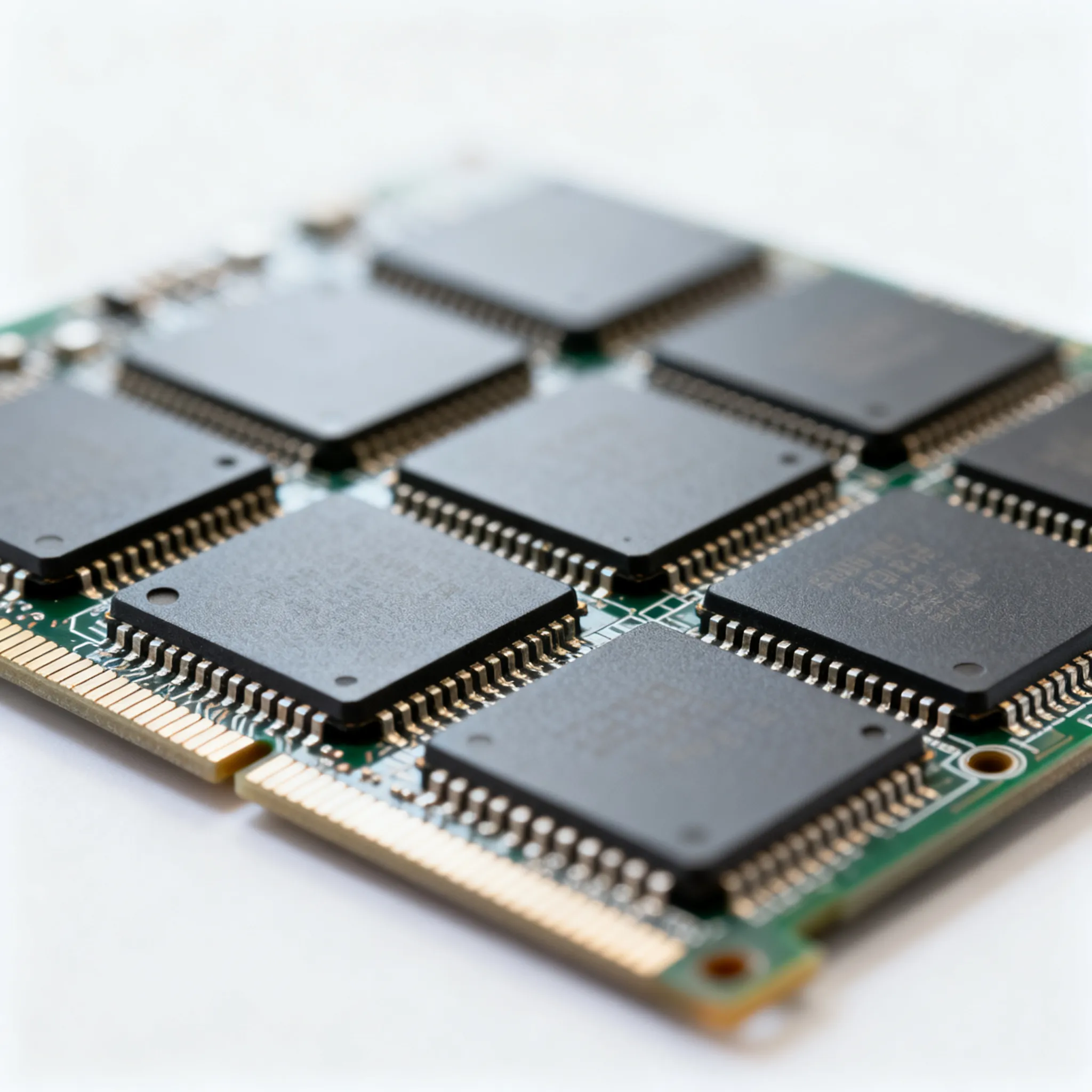
SMT Assembly
Surface-Mount Technology (SMT) lets you place tiny parts on your board quickly and accurately. You use pick-and-place machines that can set up to 25,000 parts per hour. Four machines working together can place 100,000 parts every hour. This speed means you finish more boards in less time.
Automation in SMT boosts your first-run yield from 70% to 97%. You see fewer mistakes and less rework. SMT also lets you use smaller parts and fit more on each board. This method lowers your costs and increases your output.
SMT lines use automated inspection to catch errors early. This keeps your boards reliable and your process efficient.
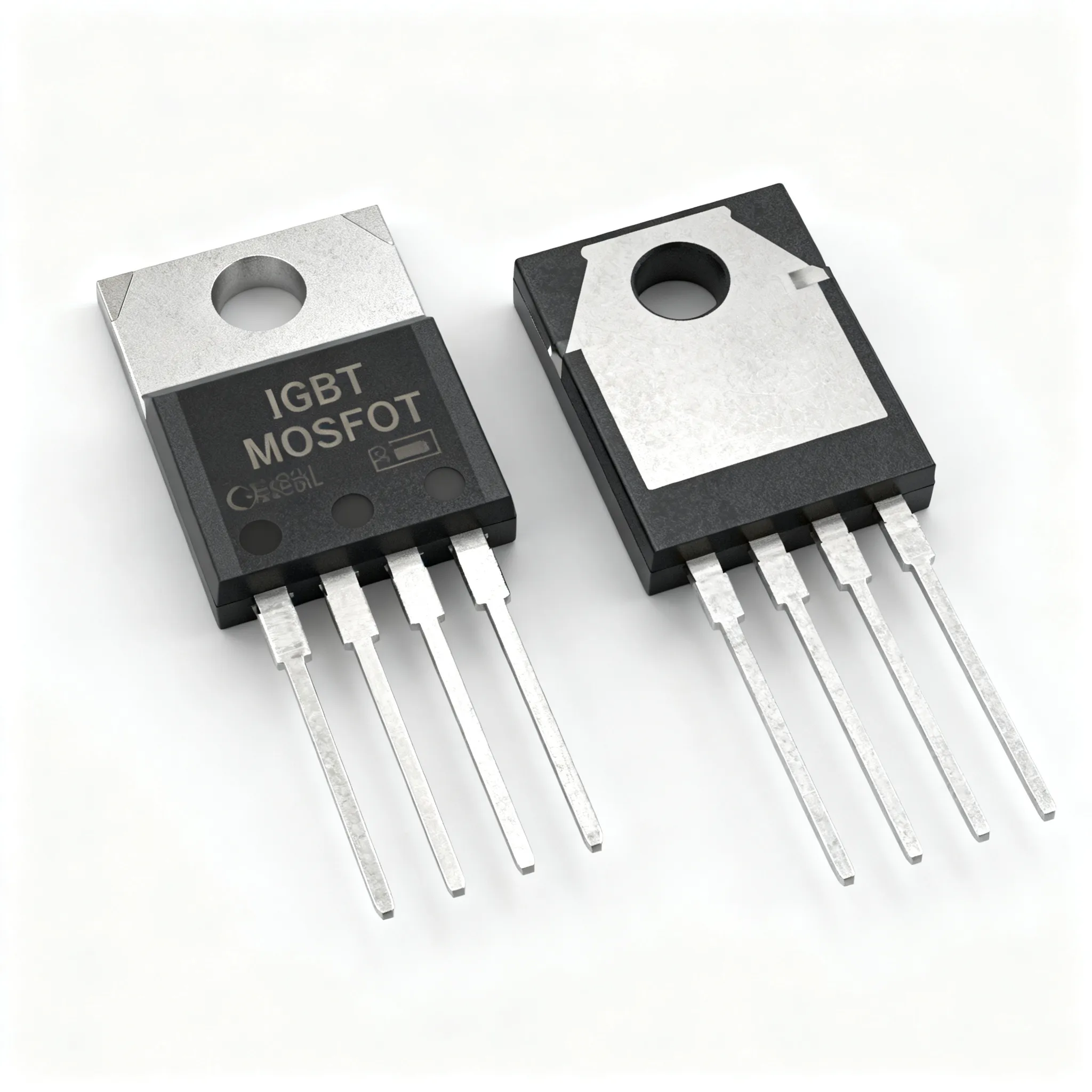
Through-Hole Assembly
Some parts need strong connections or must handle more power. You use through-hole assembly for these. You insert each part’s leads into holes on the board. Machines or skilled workers then solder the leads in place. This method gives you strong joints that hold up under stress.
You often use through-hole for connectors, switches, or large parts. It takes more time than SMT, but it adds strength where you need it most.
Soldering
Soldering joins your parts to the board. You use heat to melt solder, which flows around the leads and pads. Good soldering makes strong, reliable connections. You can use wave soldering for many through-hole parts at once or reflow soldering for SMT parts.
You check your solder joints for smoothness and shine. Dull or cracked joints can cause failures. Automated inspection tools help you spot problems fast.
Collecting data on defect rates and cycle times helps you improve your soldering process. You can use control charts to watch for changes and fix issues before they grow.
Cleaning
After soldering, you clean your board to remove flux and other residues. Clean boards last longer and work better. You may use a two-stage cleaning process: first a solvent wash, then a rinse with deionized water. This method works well for high-reliability boards, such as those used in military equipment.
-
You must remove both ionic (salts) and non-ionic (oils) contaminants.
-
Surface energy should reach at least 38 dynes/cm to ensure coatings stick well.
-
Measuring ionic contamination in micrograms per square centimeter helps you check cleaning quality.
If you skip cleaning, you risk problems like corrosion, short circuits, or coating failures.
Conformal Coating
You finish assembly by adding a conformal coating. This thin, clear layer protects your board from moisture, dust, and chemicals. Acrylic coatings are popular and cover about half the market. They help your board last longer and reduce repair costs.
-
Conformal coatings shield your board from moisture, static, and pollution.
-
They prevent corrosion and keep dust or oils from causing shorts.
-
The coating also guards against vibration and high temperatures.
Tests show that boards with conformal coating resist humidity and keep working even in tough conditions. You must choose the right coating and apply it carefully for the best protection.
Note: Always check coating adhesion and use safe removal methods if you need to repair the board later.
Testing
AOI
You use Automated Optical Inspection (AOI) to check your boards for defects after assembly. AOI machines scan each PCB and compare it to the correct design. These systems find missing parts, wrong placements, and soldering problems. AOI works much faster and more accurately than manual checks. You catch most errors early, which saves time and money. AOI helps you keep your PCB Manufacturing process reliable and efficient.
In-Circuit Test
You perform in-circuit tests (ICT) to check each component on the board. ICT uses special probes to touch test points and measure values like resistance, voltage, and current. You can spot open circuits, shorts, and faulty parts right away. This step helps you make sure every part works as it should before moving to the next stage. ICT gives you confidence that your board meets design requirements.
Functional Test
You run functional tests to see if your board works in real-world conditions. You check both mechanical and electrical features. You also test the firmware to make sure it runs correctly. Here are some things you measure during functional testing:
-
Design integrity and technical performance
-
Detection of assembly or soldering issues
-
Firmware operation and correctness
-
Signal actuation, like pressing a button to light an LED
-
Time-based and analog waveforms
-
Serial communication, such as I2C or SPI
-
Feature demonstrations and performance benchmarks
You use tools like oscilloscopes and multimeters to check these results. Functional testing ensures your board meets all performance standards before shipping.
Final Inspection
You finish with a final inspection to confirm quality. You look for any defects that earlier steps missed. Quality improvements in PCB Manufacturing have made a big difference. The table below shows how defect rates dropped after better controls:
|
Time Period |
Defect Rate (%) |
Lot Reject Rate (PPM) |
|---|---|---|
|
Before quality improvements (Nov 2021 - Mar 2022) |
~0.87 - 0.97 |
5500 |
|
After quality improvements (Apr 2022 - Sep 2022) |
0.08 - 0.19 |
900 |
You see that strong inspection steps lead to fewer defects and higher reliability. Careful testing and inspection help you deliver boards that work every time.
Delivery
Packaging
You want your finished PCBs to arrive in perfect condition. Packaging plays a big role in this final step. Manufacturers use special materials to protect your boards from dust and physical damage. They often seal each board, much like vacuum packing, to keep out moisture and dirt. After sealing, workers place the PCBs into sturdy containers that shield them from bumps and drops during transport.
To make sure the packaging works, companies follow strict standards. One important standard is ASTM D6344. This test checks if the packaging can protect your boards from impacts that happen during shipping and handling. The test uses tools like a hemispherical mass tip and pendulum to hit the package in ways that copy real-world accidents. The test focuses on the parts of the package most likely to get hit. If the packaging passes, you know your boards have a better chance of arriving safely.
Here are some key points about PCB packaging:
-
Sealed packaging keeps out dust and moisture.
-
Containers protect against physical shocks.
-
ASTM D6344 testing checks for impact resistance.
-
Testing can adjust for different package sizes and shapes.
Tip: Always ask your manufacturer about their packaging and testing methods. This helps you avoid damage and costly returns.
Shipping
Once your PCBs are packed, shipping begins. You choose a shipping method based on speed, cost, and destination. Air freight works best for urgent orders. Sea or ground shipping costs less for large or heavy shipments. Tracking systems let you follow your package from the factory to your door.
You should check the shipping company’s track record for safe delivery. Reliable carriers handle packages with care and offer insurance for added peace of mind. Good shipping practices reduce the risk of delays or damage.
|
Shipping Method |
Speed |
Cost |
Best For |
|---|---|---|---|
|
Air Freight |
Fastest |
Highest |
Urgent, small batches |
|
Sea Freight |
Slow |
Lowest |
Large, heavy shipments |
|
Ground |
Moderate |
Moderate |
Regional deliveries |
Note: Always inspect your boards when they arrive. Report any damage right away to start the claims process quickly.
You guide your project through each stage of PCB Manufacturing, from design to delivery. Careful planning, precise fabrication, and thorough assembly help you avoid costly mistakes. Testing methods like Accelerated Life Testing and X-ray Inspection confirm your boards meet high standards. When you use best practices, you see fewer defects and better performance. Review your process often or work with experienced manufacturers to get reliable, high-quality PCBs.
FAQ
What is the difference between SMT and through-hole assembly?
SMT places parts directly on the board’s surface. Through-hole assembly puts part leads through holes in the board. SMT works well for small parts and fast production. Through-hole gives stronger connections for large or heavy parts.
How do you choose the right PCB material?
You match the material to your project’s needs. FR4 works for most electronics. For high heat or special uses, you pick advanced materials like CF 004. Always check the material’s strength, cost, and performance.
Why is AOI important in PCB manufacturing?
AOI, or Automated Optical Inspection, finds defects early. You use AOI to check for missing parts, wrong placements, or soldering problems. This step helps you catch mistakes before they cause bigger issues.
How can you avoid common PCB design mistakes?
You run design rule checks and follow your manufacturer’s guidelines. Double-check your files before sending them out. Use prototyping to test your design. Good communication with your team also helps prevent errors.
What should you do if your PCBs arrive damaged?
You inspect the boards as soon as they arrive. Take photos of any damage. Contact your supplier right away and start the claims process. Good packaging and reliable shipping reduce the risk of damage.