

2SC2712 Datasheet and Pinout: Specs for Design and Sourcing
2SC2712 datasheet essentials, pinout overview, key specs, and design/sourcing checks for engineers and buyers. Request a quote on IC-Online.
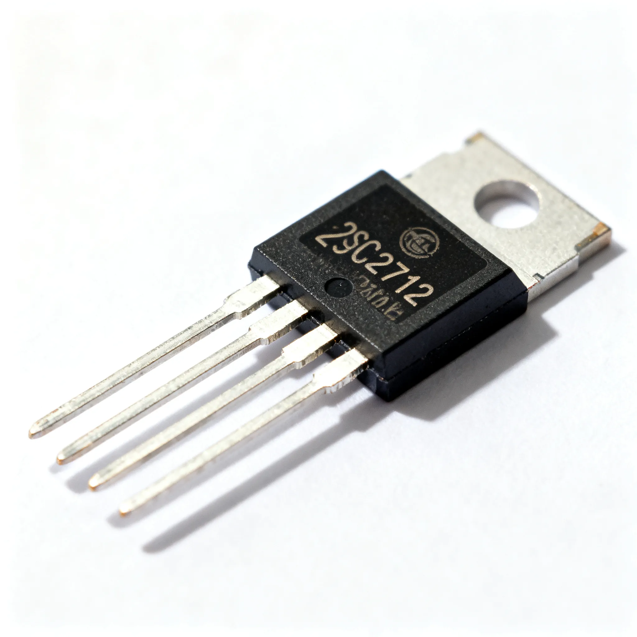
Why the 2SC2712 Remains a Go-To Low-Noise NPN Transistor — and the Sourcing Realities
When a design calls for a low-noise, small-signal NPN transistor in a surface-mount package, the 2SC2712 consistently rises to the top of the shortlist. Introduced by Toshiba and built on their proprietary PCT (Pure Complementary Transistor) process, this silicon NPN epitaxial device carved out a reputation in audio-frequency amplification where signal integrity is non-negotiable. The standout figure on its datasheet — a noise figure (NF) of just 1 dB typical at 1 kHz — places it among the quietest commodity bipolar transistors available in a SOT-23 footprint. Coupled with a collector-emitter voltage rating of 50 V and a collector current capacity of 150 mA, the part comfortably handles the voltage swings and drive requirements encountered in preamplifier stages, microphone input buffers, and line-level signal chains.
But the 2SC2712's longevity in production has created a sourcing landscape that rewards careful engineering scrutiny. Toshiba's original device — documented in the official Toshiba 2SC2712 datasheet (2014 revision) — specifies three hFE gain grades (O, Y, GR) with tightly controlled linearity across a two-decade collector current range. However, multiple second-source manufacturers now produce transistors bearing the "2SC2712" marking, including Unisonic Technologies (UTC) and Galaxy Microelectronics. The alltransistors.com 2SC2712 equivalent finder catalogs these alternatives and cross-references JEDEC-registered parts that may be evaluated for compatibility.
Key Takeaway: The same part number can mask meaningful differences in noise performance, hFE binning tolerances, and process consistency across manufacturers. Engineers integrating the 2SC2712 into a production BOM should anchor their evaluation to Toshiba's original datasheet parameters and treat alternative-source versions as candidates requiring qualification — not as compatibility must be verified (package, pinout, firmware) equivalents. For procurement teams, the multi-source reality means availability can be managed across suppliers, but each source must be validated against the target specifications before approval.
Designers who gravitate toward this device typically cite three characteristics: the excellent hFE linearity — with a ratio of hFE at 0.1 mA to hFE at 2 mA specified at 0.95 typical — that minimizes distortion in small-signal amplification; the combination of 50 V VCEO and 150 mA IC in a SOT-23 package that handles real-world audio headroom; and the 1 dB noise floor that eliminates the transistor as a meaningful contributor to system hiss. These parameters, verified against the manufacturer's documentation available on alldatasheet.com's Toshiba 2SC2712 page, form the baseline against which all alternatives should be measured.
Decoding the 2SC2712 Pinout and Absolute Maximum Ratings
Before placing a single 2SC2712 on a PCB layout or committing a BOM line to procurement, engineers need to lock in two fundamentals: the pinout orientation and the absolute maximum envelope the device can tolerate. The SOT-23 (also designated SC-59 or TO-236) package used by this transistor follows a standard three-terminal configuration, but pin assignments are not universal across all small-signal transistors — and a swapped base-emitter connection will render a low-noise stage inoperative on first power-up.
Per the Toshiba 2SC2712 datasheet, the SOT-23 pin map is as follows:
- Pin 1 — Base: The control terminal; bias voltage applied here modulates collector current.
- Pin 2 — Emitter: Typically connected to ground or the negative rail in common-emitter topologies.
- Pin 3 — Collector: The output terminal; connects to the supply rail through a load resistor in common-emitter configurations.
Holding the device with the flat face toward you and pins facing downward, pin 1 is the leftmost terminal, pin 2 is the center, and pin 3 is the rightmost. This orientation is consistent across Toshiba, UTC, and Galaxy Microelectronics versions — a helpful convergence that reduces footprint risk when qualifying second sources. However, always confirm against the specific manufacturer's datasheet; the Unisonic 2SC2712 datasheet and the Galaxy Microelectronics 2SC2712 datasheet both maintain this pin assignment, but verification is a zero-cost insurance policy.
The absolute maximum ratings define the destruction boundaries. Exceeding any single parameter — even momentarily during startup transients or fault conditions — risks permanent degradation or catastrophic failure. The table below consolidates these limits from the Toshiba datasheet:
| Parameter | Symbol | Rating | Unit | Conditions |
|---|---|---|---|---|
| Collector-Base Voltage | VCBO | 60 | V | Emitter open |
| Collector-Emitter Voltage | VCEO | 50 | V | Base open |
| Emitter-Base Voltage | VEBO | 5 | V | Collector open |
| Collector Current | IC | 150 | mA | DC continuous |
| Base Current | IB | 50 | mA | DC continuous |
| Collector Power Dissipation | PC | 150 | mW | Ta = 25°C, FR-4 board |
| Junction Temperature | Tj | 125 | °C | — |
| Storage Temperature Range | Tstg | -55 to +125 | °C | — |
Design Note: The 150 mW power dissipation rating assumes standard FR-4 PCB mounting at 25°C ambient. In enclosed audio equipment where internal temperatures routinely reach 50–60°C, derate the allowable dissipation by approximately 1.2 mW/°C above 25°C. At 60°C ambient, safe dissipation drops to roughly 108 mW — still comfortable for most small-signal stages operating at IC = 1–2 mA and VCE = 5–10 V, but worth calculating before finalizing a layout that places the device near hot voltage regulators or power amplifier heatsinks.
Beyond the absolute maxima, the 2SC2712's electrical characteristics table is where design decisions crystallize. The transition frequency (fT) of 80 MHz confirms wideband capability far beyond audio's 20 kHz ceiling, but its real significance lies in maintaining low base spreading resistance — a contributor to the device's low noise. The hFE classification system splits production into three bins: O (70–140), Y (120–240), and GR (200–400). The hFE linearity specification — guaranteeing that gain at 0.1 mA collector current stays within 5% of gain at 2 mA — is the parameter that separates this device from general-purpose transistors. In a common-emitter preamplifier stage where signal swings modulate instantaneous collector current, a flat hFE curve translates directly to low total harmonic distortion.
| Electrical Characteristic | Symbol | Min | Typ | Max | Unit | Test Conditions |
|---|---|---|---|---|---|---|
| Collector Cut-off Current | ICBO | — | — | 0.1 | µA | VCB = 60 V, IE = 0 |
| DC Current Gain (O grade) | hFE | 70 | — | 140 | — | VCE = 6 V, IC = 2 mA |
| DC Current Gain (Y grade) | hFE | 120 | — | 240 | — | VCE = 6 V, IC = 2 mA |
| DC Current Gain (GR grade) | hFE | 200 | — | 400 | — | VCE = 6 V, IC = 2 mA |
| hFE Linearity Ratio | hFE(0.1mA) / hFE(2mA) | — | 0.95 | — | — | VCE = 6 V |
| Transition Frequency | fT | — | 80 | — | MHz | VCE = 10 V, IC = 1 mA |
| Collector Output Capacitance | Cob | — | 3.5 | 7.0 | pF | VCB = 10 V, f = 1 MHz |
| Noise Figure | NF | — | 1 | 10 | dB | VCE = 6 V, IC = 0.1 mA, Rg = 10 kΩ, f = 1 kHz |
The noise figure specification deserves careful reading. The typical 1 dB NF is measured at a source resistance of 10 kΩ — a value representative of many audio preamplifier input networks. At lower source impedances or higher collector currents, the noise figure will shift. The 10 dB maximum bound exists to accommodate worst-case process variation; production testing typically yields devices clustered near the typical value, but the datasheet's max limit establishes the guardrail that should be used for worst-case signal-to-noise ratio budgeting in production designs.
2SC2712 Variants and Equivalent Transistors: How They Stack Up
The 2SC2712 designation no longer points to a single silicon die from a single fabrication line. Toshiba remains the reference standard, but the part number has been adopted by multiple manufacturers whose devices share the same functional footprint while diverging on parameters that matter in precision analog circuits. Engineers evaluating cost-reduction opportunities or second-sourcing strategies need a clear-eyed comparison — not assumptions of interchangeability.
The cross-reference tool at alltransistors.com identifies the Toshiba original alongside JEDEC-registered alternatives such as the KSC2712 from ON Semiconductor (formerly Fairchild). The Unisonic Technologies version, documented in their 2SC2712 datasheet, and the Galaxy Microelectronics implementation, available in the GME 2SC2712 datasheet, represent the most commonly encountered alternatives in distributor channels.
Tip: When qualifying a second-source 2SC2712, request the full datasheet — not just a summary page — and compare the noise figure test conditions, hFE binning ranges, and the presence (or absence) of an hFE linearity specification. A part that matches on VCEO, IC, and package but omits the linearity guarantee may exhibit higher distortion in real amplifier stages.
| Parameter | Toshiba 2SC2712 (Reference) | Unisonic (UTC) 2SC2712 | Galaxy Microelectronics 2SC2712 | KSC2712 (ON Semi) — Cross-Ref Candidate |
|---|---|---|---|---|
| VCEO (max) | 50 V | 50 V | 50 V | 50 V |
| IC (max) | 150 mA | 150 mA | 150 mA | 150 mA |
| PC (max, Ta=25°C) | 150 mW | 200 mW | 200 mW | 150 mW (verify with mfr. datasheet) |
| fT (typ.) | 80 MHz | 80 MHz | 80 MHz | 80 MHz |
| NF (typ. at 1 kHz) | 1 dB (Rg=10kΩ, IC=0.1mA) | 1 dB (verify test conditions) | Specification not explicitly listed | Verify on ON Semi datasheet |
| hFE Grades Available | O, Y, GR | O, Y, GR | O, Y, GR | O, Y, GR (confirm bin limits) |
| hFE Linearity Spec | 0.95 typ. (ratio at 0.1mA/2mA) | Not explicitly specified | Not explicitly specified | Verify on manufacturer datasheet |
| Package | SOT-23 (SC-59) | SOT-23 | SOT-23 | SOT-23 |
Reading the comparison: The power dissipation rating of 200 mW claimed by UTC and Galaxy is an incremental advantage for designs operating at elevated ambient temperatures, but it does not compensate for the missing hFE linearity specification. If your circuit topology relies on the transistor's gain remaining constant across a dynamic current range — common in class-A preamplifier stages with resistive loads — the Toshiba original's documented linearity provides a design margin that alternative sources may not guarantee, even if typical performance is comparable. The noise figure gap is equally significant: Galaxy's datasheet does not explicitly list an NF parameter, which means any low-noise design using that version is operating without a manufacturer-backed noise guarantee. For audio-grade procurement, buyers should require the specific manufacturer's noise figure test report or confirm the parameter via incoming inspection before approving a second source.
The KSC2712 from ON Semiconductor appears in the alltransistors cross-reference as a JEDEC-registered equivalent and offers another sourcing path. However, the same verification discipline applies: request the ON Semi datasheet, compare noise figure test conditions against the Toshiba baseline, and run a sample qualification in-circuit before committing a production BOM change. No cross-reference tool — however authoritative — substitutes for bench validation when signal integrity is at stake.
Practical Design and Sourcing Tips for the 2SC2712
Integrating the 2SC2712 into a production-ready design involves converging the engineering requirements — bias points, noise floor, layout — with the procurement realities of multi-source qualification, authorized distribution, and incoming inspection criteria. The following guidance bridges both domains.
Biasing According to hFE Grade
The choice of O, Y, or GR grade is not arbitrary; it should be driven by the target collector current and the available base drive in your circuit topology. For low-current preamplifier input stages operating at IC = 0.1–0.5 mA, the GR grade (hFE = 200–700) provides high gain with minimal base current draw, reducing loading on high-impedance sources such as condenser microphone capsules or magnetic phono cartridges. The O grade (hFE = 70–140), with its tighter and lower gain band, suits stages where consistent, moderate gain simplifies production calibration — such as line-level buffer amplifiers where signal levels are already substantial and gain variation across units must be minimized.
Design Rule of Thumb: Calculate the base resistor for the minimum specified hFE in the selected grade bin, not the typical value. A GR-grade device with a datasheet minimum of 200 operating at IC = 1 mA and VCC = 12 V requires a base resistor selected for hFE = 200; if a particular device exhibits hFE = 600, the circuit will saturate the transistor more heavily but will not risk damage or nonlinearity in a well-designed common-emitter stage with adequate collector load resistance.
Preserving the 1 dB Noise Figure in Layout
A transistor specified for 1 dB typical noise figure can easily deliver 6–8 dB in a poorly executed PCB layout. The noise floor of the 2SC2712 is low enough that layout parasitics — ground loops, shared return paths, capacitive coupling from digital traces — dominate the system noise budget. Key layout considerations include:
- Star-ground the emitter return: Route the emitter resistor's ground connection directly to the system's quiet analog ground node; do not share a return trace with decoupling capacitors from noisy digital or power-supply sections.
- Minimize base lead length: The base terminal is the most noise-sensitive node. Place the input coupling capacitor and bias resistors within 5 mm of the base pin, and avoid routing high-impedance base traces parallel to clock lines or switching regulator nodes.
- Guard rings for high-impedance nodes: If the base is driven from a source impedance exceeding 10 kΩ, consider a guard ring connected to a low-impedance reference (emitter or ground) around the base trace to divert leakage currents.
- Shield sensitive stages: In multi-channel audio equipment, a grounded copper pour or shield can surrounding the first gain stage prevents capacitive crosstalk from adjacent channels from degrading the effective noise figure.
Procurement Workflow for Stable Supply
On the sourcing side, the 2SC2712 is carried by authorized distributors including Mouser Electronics, which stocks the Toshiba-manufactured version. For procurement teams managing production BOMs, the following workflow reduces supply risk without compromising specification compliance:
- Anchor the approved vendor list to Toshiba: Designate the Toshiba original as the primary source and lock the specification set to the official Toshiba datasheet.
- Qualify one alternate source proactively: Select either the UTC or Galaxy Microelectronics version and run a formal qualification — including noise figure measurement at the target IC and source impedance — before a shortage forces a rushed substitution.
- Include datasheet revision tracking in the BOM: Record the datasheet revision date and manufacturer for every approved source so that incoming inspection can flag parameter changes.
- Require date-code documentation: Buyers should specify a maximum date-code age (e.g., within 36 months of shipment) and request a Certificate of Conformance that maps the shipment to the manufacturer's lot traceability records.
- Use cross-reference tools for spot-buy flexibility: The alltransistors.com equivalent finder identifies additional JEDEC-registered parts such as the KSC2712 that can be evaluated as emergency alternatives, with full bench validation required before approval.
| Sourcing Consideration | Recommended Action | Risk If Skipped |
|---|---|---|
| Manufacturer Verification | Request datasheet with manufacturer logo and revision date; cross-check marking format against datasheet | Third-party part may lack hFE linearity or noise figure guarantees |
| hFE Grade Confirmation | Verify the suffix (O, Y, GR) on the part marking and packing slip matches the BOM requirement | Wrong gain grade shifts bias points and may cause clipping or excessive noise |
| Noise Figure Validation | For low-noise designs, require spot-check NF measurements on incoming samples at the design's IC and source impedance | Unverified parts may deliver 6–10 dB NF, degrading system SNR |
| Multi-Source Qualification | Bench-test at least one alternative manufacturer's version under worst-case conditions (temperature, VCC tolerance) | Single-source dependency creates line-down risk during allocation periods |
| Distributor Authorization | Source Toshiba parts through authorized distributors; request traceability documentation | Counterfeit or relabeled parts may fail prematurely or deviate from published specs |
These sourcing practices apply equally whether you are purchasing 1,000 pieces for a production run or 50,000 pieces under an annual contract. The disciplined approach — datasheet-anchored qualification, documented traceability, and proactive second-source evaluation — ensures that the 2SC2712 on your BOM delivers the performance your design demands, regardless of which authorized manufacturer fills the order.
2SC2712 Design and Procurement FAQ: Answers for Experienced Engineers and Buyers
Q: How do I distinguish a genuine Toshiba 2SC2712 from a third-party or counterfeit part by marking?
Genuine Toshiba 2SC2712 parts carry a laser-marked code on the flat face of the SOT-23 package that includes the hFE grade suffix — 'O', 'Y', or 'GR' — as specified in the official Toshiba datasheet. The marking format, character font, and position are consistent with Toshiba's SOT-23 marking standard. Third-party manufacturers such as UTC and Galaxy Microelectronics reuse the '2SC2712' designation and may employ similar marking conventions, so visual inspection alone cannot distinguish the silicon inside. The most reliable verification method is to request the specific manufacturer's datasheet — matching the lot code and date code to the supplier's documentation — and to source Toshiba-manufactured devices through their authorized distribution network. For high-value or safety-critical designs, incoming inspection with a curve tracer or semiconductor parameter analyzer can verify key parameters against the Toshiba datasheet's typical and maximum limits.
Q: Can I replace a 2SC2712 with a BC847 or 2N3904 in a low-noise preamplifier?
Not without accepting a measurable noise penalty. The 2SC2712's noise figure of 1 dB typical (at 1 kHz, Rg = 10 kΩ, IC = 0.1 mA) is superior to the BC847's typical noise performance in the 3–4 dB range under similar bias conditions. For a condenser microphone preamplifier or moving-magnet phono stage where every decibel of signal-to-noise ratio matters, substituting a general-purpose BC847 will raise the noise floor audibly. The 2N3904 introduces an additional complication: it is predominantly available in the through-hole TO-92 package, making it physically incompatible with SOT-23 footprints without a board respin. If you need a surface-mount alternative, use the alltransistors.com cross-reference to identify SOT-23 candidates such as the KTC2712 or KSC2712, then verify the noise figure specification on the candidate's datasheet against your circuit's operating conditions before committing to a substitution.
Q: What's the practical significance of the hFE linearity spec (hFE ratio = 0.95) for circuit design?
The hFE linearity specification — the ratio of DC current gain measured at IC = 0.1 mA to the gain at IC = 2 mA, with a typical value of 0.95 on the Toshiba datasheet — quantifies how flat the transistor's gain remains across a 20:1 collector current range. In a common-emitter amplifier with a resistive load, the instantaneous collector current varies as the input signal modulates the base voltage. If hFE drops significantly at lower currents, the amplifier's gain becomes signal-dependent, introducing distortion products that manifest as harmonic content in the output. The 2SC2712's 0.95 ratio means gain varies by only 5% across that two-decade span, minimizing this distortion mechanism. For the design engineer, this linearity simplifies biasing: you can confidently set the DC operating point using the minimum hFE value for the selected grade (O, Y, or GR) without extensive characterization of gain variation across the expected signal swing. Choose the O grade for very low-current stages (IC < 0.5 mA) where its tighter gain band reduces unit-to-unit variation, and the GR grade for stages needing higher transconductance at IC = 1–2 mA.
Q: I need to source 2SC2712 in volume with a stable supply. What's the lead time and which authorized distributors stock it?
The 2SC2712 from Toshiba is stocked by authorized distributors including Mouser Electronics. Rather than relying on fixed lead-time numbers — which fluctuate with fab loading, allocation cycles, and regional demand — buyers should confirm allocation-backed lead time with the supplier at the time of RFQ. For high-volume procurement, qualifying a second source such as the Unisonic (UTC) or Galaxy Microelectronics version provides supply flexibility, but note that noise specifications and hFE linearity parameters may differ from the Toshiba original. Use the alltransistors.com equivalent finder to identify JEDEC-registered alternatives like the KSC2712 from ON Semiconductor, which expands the pool of authorized distributors. A structured procurement approach — primary source locked to Toshiba with one qualified alternate, periodic RFQs to test market availability, and documented incoming inspection criteria — provides the most reliable supply strategy without compromising the low-noise performance your design requires.
Q: How critical is the 80 MHz fT for audio applications, and will a transistor with lower fT cause phase issues?
For audio-frequency amplification with a bandwidth ceiling of 20 kHz, the 2SC2712's 80 MHz transition frequency is far in excess of what phase-response considerations demand. Even a transistor with fT = 10 MHz provides sufficient gain-bandwidth product to maintain flat closed-loop response and negligible phase shift within the audio band in a properly compensated amplifier stage. The 80 MHz fT of the 2SC2712 is not selected for its phase margin contribution; rather, it is a by-product of the shallow, optimized base doping profile that also delivers the 1 dB noise figure. A higher fT correlates with lower base spreading resistance (rbb'), which directly reduces thermal noise generation in the base region. If you substitute a BC847 — which coincidentally also has an fT around 100 MHz — you will maintain adequate phase performance in the audio band, but you are almost certain to sacrifice the 2SC2712's noise figure and hFE linearity, as those parameters are independently optimized and not guaranteed by the BC847's process. In short: fT is a proxy for process quality, not a direct audio requirement, but swapping based solely on fT equivalence fails to address the parameters that make this transistor valuable in low-noise designs.
References & Further Reading
- Toshiba 2SC2712 Official Datasheet (2014-03-01 Revision) — Primary reference for electrical characteristics, absolute maximum ratings, and package dimensions.
- Toshiba 2SC2712 Datasheet on Alldatasheet — Archived datasheet access for Toshiba's Audio Frequency General Purpose Amplifier NPN Transistor.
- 2SC2712-GR Equivalent Finder and Cross-Reference on AllTransistors — Cross-reference database for identifying compatible transistors and JEDEC-registered alternatives.
- Unisonic Technologies (UTC) 2SC2712 Datasheet — Second-source datasheet from Unisonic Technologies; compare noise figure and hFE linearity specifications against the Toshiba original.
- ← Previous ArticleNext Article >>
Related Articles
 Blog
BlogWhat Does a Resonator Do
What does a resonator do? It generates and stabilizes a specific frequency for timing, signal generation, and filtering in electronic circuits.
 Blog
BlogCS8575S Supply Risk Assessment: What to Ask Before You Buy
Assess CS8575S sourcing risks before you buy. RFQ questions on traceability, date codes, testing, alternatives, and supply continuity for procurement teams.
 Blog
BlogUnderstanding How Graphics Cards Work in Ordinary Electronics
A definition graphics card explains how this hardware turns data into images for your screen. It's crucial for video calls, streaming, and light gaming on daily devices.
 Blog
BlogUnderstanding DC Circuits and Their Practical Uses
What is a dc circuit? It's a closed loop with constant voltage and unidirectional current, powering everyday electronics. See its practical uses in electronics.
 Blog
Blog776230-1 Datasheet and Pinout: Specs for Design and Sourcing
776230-1 datasheet essentials, pinout overview, key specs, and design/sourcing checks for engineers and buyers. Request a quote on IC-Online.
 Blog
BlogMBR30150CT Supply Risk Assessment: What to Ask Before You Buy
Assess MBR30150CT sourcing risks before you buy. RFQ questions on traceability, date codes, testing, alternatives, and supply continuity for procurement teams.