3313J-1-102E Datasheet, Pinout, and Specs for Engineers
3313J-1-102E datasheet essentials, pinout overview, key specs, and design/sourcing checks for engineers and buyers. Request a quote on IC-Online.
3313J-1-102E Datasheet, Pinout, and Specs for Engineers
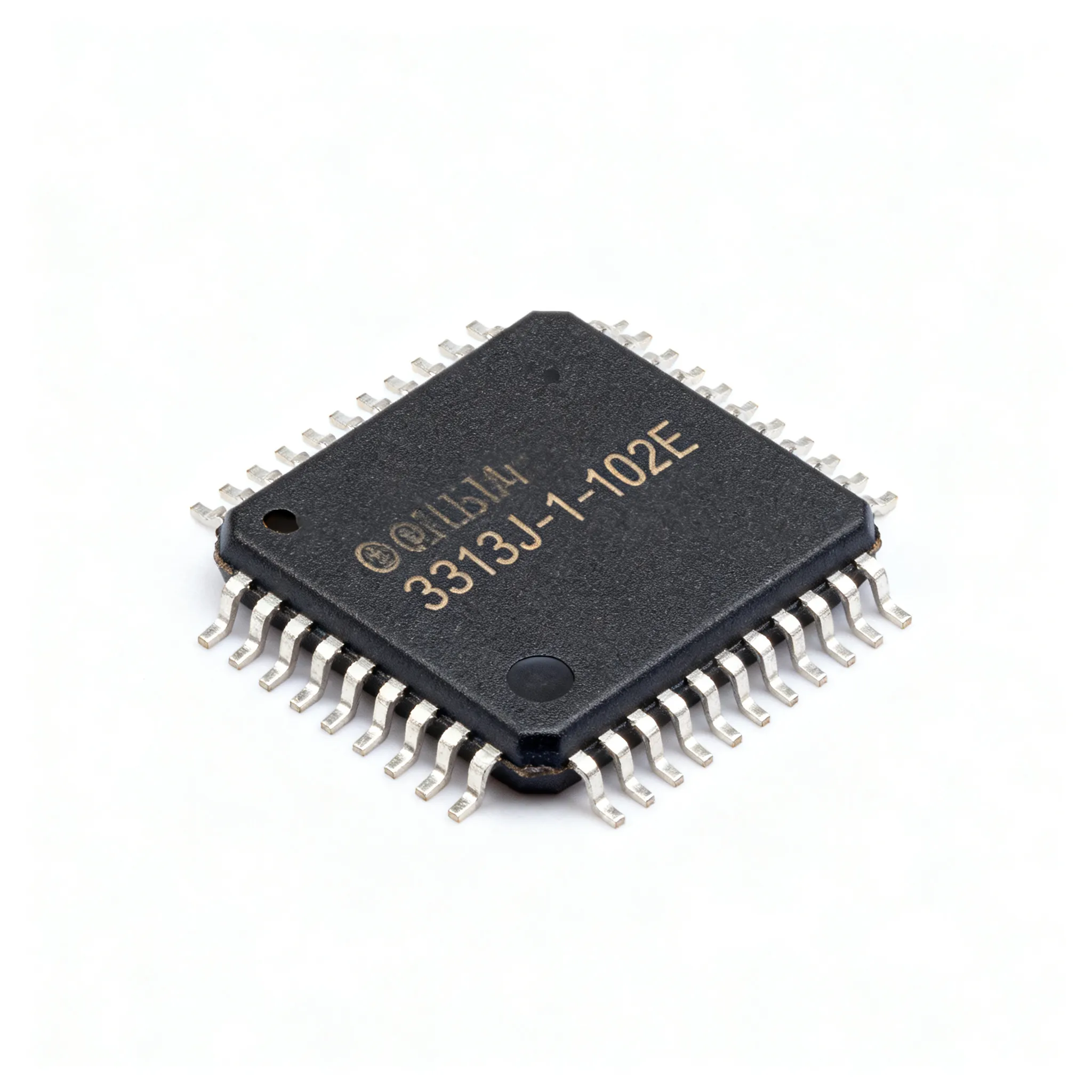
The 3313J-1-102E from Bourns is a 1 kΩ single‑turn cermet trimmer potentiometer that engineers keep reaching for when they need a compact, surface‑mount calibration node. With a 3.2 × 3.5 mm footprint and J‑lead gull‑wing terminals, it slips into dense analog front‑ends, sensor interfaces, and bias networks without stealing board real estate. But sourcing it isn’t always a one‑click exercise. Some distributor portals gate access behind account logins, and stock levels can shift rapidly across the usual channels. This article unpacks the datasheet essentials, pinout, footprint, and procurement techniques that help you integrate the 3313J-1-102E into production without last‑minute surprises.
Why the 3313J-1-102E Keeps Appearing in BOMs — and Where Sourcing Gets Tight
The Bourns 3313J-1-102E isn’t a high‑dollar chip; it’s a $0.585 trimmer that solves a stubborn analog problem. Engineers use it to dial out offset voltages, fine‑tune gain, or set a reference level in a voltage divider. Because it’s cermet, it survives reflow without the drift that carbon‑film trimmers can exhibit after thermal cycling. The single‑turn mechanical design is coarse enough for fast lab tweaks yet fine enough for many production calibration steps.
Still, the 3313J-1-102E can cause procurement friction. Some distributors, such as TTI, restrict online pricing and availability to account holders — a barrier that complicates instant BOM cost‑out TTI access limitation. Meanwhile, LCSC, DigiKey, and JLCPCB may show healthy inventory one day and low stock the next, because the part is used in high‑volume industrial and instrumentation designs. Those fluctuations make it wise to cross‑check multiple sources and treat allocation as dynamic. When you’re qualifying a BOM for a long‑life product, verifying distributor availability through a single‑point‑of‑contact or an RFQ channel reduces the risk of a line‑stop.
Tip: Even though the 3313J-1-102E is a standard Bourns catalog item, do not assume unlimited supply. Build a sourcing strategy that includes at least two independent distributors and a factory‑authorized partner. Confirm allocation‑backed lead time through an RFQ rather than relying on a web‑store stock indicator.
Inside the 3313J-1-102E: Pinout, Footprint, and the Datasheet Numbers That Matter
The 3313J-1-102E is a three‑terminal device with a classic potentiometer topology. Viewed from the top, the three J‑lead pins are arranged in a triangle: the two outer terminals are the fixed ends of the resistive element, and the center terminal is the wiper. Pin 1 and Pin 3 are the end terminals; Pin 2 is the wiper. The wiper moves clockwise when the adjustment screw is turned from the top, increasing the resistance between Pin 1 and the wiper while decreasing it between the wiper and Pin 3. This straightforward layout means you can use it as a variable resistor (rheostat) by connecting the wiper to one end, or as a true voltage divider.
The surface‑mount footprint is compact: 3.2 mm × 3.5 mm, with a 1.0 mm maximum height. The J‑lead shape provides a compliant solder joint that absorbs some mechanical stress, which is why the 3313J-1-102E holds up well in board‑level vibration tests. You can download a verified footprint and schematic symbol from SnapMagic, which exports to Altium, KiCad, Eagle, and other major EDA tools SnapMagic footprint and symbol. The Bourns datasheet also includes a recommended land pattern; using it is essential to avoid tombstoning during reflow.
Below is a table of key specifications pulled from the manufacturer’s datasheet and distributor listings. These are the numbers that drive reliability and thermal performance in your circuit.
| Parameter | Value/Range | Unit/Notes |
|---|---|---|
| Resistance | 1 kΩ | End-to-end |
| Resistance Tolerance | ±20% | Standard cermet trimmer tolerance |
| Temperature Coefficient (TCR) | ±100 ppm/°C | Typical for cermet |
| Power Rating | 125 mW at 70 °C | Derates to 0 W at 150 °C |
| Adjustment Type | Top adjust, single turn | Mechanical travel: 1 turn |
| Number of Terminals | 3 (J‑lead) | Gull‑wing SMD |
| Package Dimensions | 3.2 mm × 3.5 mm × 1.0 mm max | EIA 3216 metric |
| Operating Temperature Range | –55 °C to +125 °C | Full power to 70 °C then derate |
| RoHS Compliance | Yes | Per Bourns declaration |
| Adjustment Screw Torque | ≤ 1.0 N·m | Exceeding may damage element |
These specifications are drawn from the Bourns datasheet available through LCSC and other distributors LCSC datasheet. The ±20% tolerance might look loose, but remember that it applies to the absolute end‑to‑end resistance. In a voltage divider or rheostat configuration, the ratio adjustment is what matters, and that can be tuned out during calibration. The TCR of ±100 ppm/°C is typical for a cermet element and is adequate for most industrial and consumer applications. For precision reference circuits, you’ll need to account for the 1 kΩ variant’s drift contribution in your error budget.
Side-by-Side: 3313J-1-102E vs. Alternative SMD Trimmers for 1kΩ Adjustments
When the 3313J-1-102E is unavailable or you need a different package size, engineers often evaluate other Bourns Trimpot series or equivalent Vishay parts. The table below compares the 1 kΩ 3313J-1-102E with its 10 kΩ sibling, the larger 4 mm 3314J‑1‑102E, and a Vishay TS53YL 1 kΩ trimmer. All are single‑turn, cermet, and suitable for surface‑mount reflow, but the differences in power, size, and availability can sway your decision.
| Parameter | 3313J-1-102E (Bourns) | 3313J-1-103E (Bourns, 10kΩ) | 3314J-1-102E (Bourns, 4mm) | TS53YL 1kΩ (Vishay) |
|---|---|---|---|---|
| Resistance | 1 kΩ | 10 kΩ | 1 kΩ | 1 kΩ |
| Resistance Tolerance | ±20% | ±20% | ±20% | ±20% |
| Power Rating (at 70 °C) | 125 mW | 125 mW | 250 mW | 125 mW |
| TCR | ±100 ppm/°C | ±100 ppm/°C | ±100 ppm/°C | ±100 ppm/°C |
| Package Dimensions | 3.2 × 3.5 mm | 3.2 × 3.5 mm | 4.5 × 4.5 mm | 3.0 × 3.0 mm |
| Adjustment Type | Top adjust | Top adjust | Top adjust | Top adjust |
| Termination | J‑lead | J‑lead | J‑lead | J‑lead |
| Typical 1ku Price (USD)* | $0.59 | $0.59 | $0.75 | $0.65 |
| Key Selection Note | Baseline 1kΩ trimmer; compact, widely available | Same footprint, higher resistance for lower‑current applications | Higher power handling; larger footprint | Slightly smaller footprint; alternative if Bourns allocation is tight |
*Prices are approximate and based on distributor data (LCSC, DigiKey, Octopart). Verify current pricing and availability with your supplier.
The 3313J‑1‑103E shares the identical package and pinout, so it is a drop‑in change if your circuit can accept the 10 kΩ value. The 3314J‑1‑102E doubles the power rating but requires a 4.5 mm square footprint — a significant increase that may force a board re‑spin. The Vishay TS53YL is a compelling alternative when Bourns parts are constrained, but you must verify land‑pattern compatibility because the 3.0 mm square body differs slightly from the Bourns 3.2 mm footprint. Always pull the manufacturer’s recommended land pattern and compare it to your PCB layout before substituting. Octopart provides a side‑by‑side distributor comparison for these parts Octopart distributor comparison, and DigiKey’s product page lists real‑time stock levels DigiKey part detail.
PCB Layout and Procurement Tips: Making the 3313J-1-102E Work in Production
Integrating the 3313J-1-102E into an automated SMD line involves more than dropping a footprint symbol. The J‑lead co‑planarity must be accounted for in the stencil design, and the adjustment screw needs protection from flux ingress during wave or reflow soldering. The table below captures the most critical layout and sourcing actions, drawn from manufacturer recommendations and field experience.
| Area | Recommendation | Why It Matters |
|---|---|---|
| Footprint Source | Download the verified footprint from SnapMagic or use the Bourns datasheet land pattern | Prevents tombstoning and solder opens; ensures J‑lead co‑planarity |
| EDA Library | Use the EasyEDA library for JLCPCB assembly; it maps directly to the part’s JLCPCB part number JLCPCB part entry | Streamlines fabrication and assembly without manual symbol creation |
| Power Derating | Derate linearly from 125 mW at 70 °C to 0 W at 150 °C | Avoids thermal runaway and irreversible resistance drift |
| Flux Protection | Specify a no‑clean flux process and orient the trimmer so the adjustment screw faces away from the solder wave; add a temporary Kapton tape mask if needed | Flux residue inside the screw can alter contact resistance and cause intermittent calibration |
| Pick‑and‑Place | Ensure the pick‑and‑place nozzle does not contact the adjustment screw; use a vacuum tip that grips the body only | Prevents mechanical damage that could shift the wiper position |
| Distributor Diversification | Quote the 3313J-1-102E through at least two independent distributors and one factory‑authorized partner | Reduces single‑source risk; some distributors like TTI require login, so having alternatives speeds procurement |
| Tape‑and‑Reel | Confirm the reeling orientation and quantity (e.g., 1,000‑piece reel) with your CM | Compatible with standard 8 mm tape feeders |
To avoid land‑pattern errors, always cross‑check the footprint against the Bourns recommended layout. SnapMagic provides a 3D model that you can import into your MCAD environment to check for mechanical interferences with nearby components SnapMagic CAD models. If you are using JLCPCB’s assembly service, the part is already in their library, which can eliminate the need for a custom footprint approval step.
On the procurement side, treat the 3313J-1-102E as an allocation‑sensitive part. Don’t wait until the last week before production to order. Instead, incorporate these actions into your BOM release checklist:
- Request a current allocation‑backed lead time quote from your primary distributor; do not rely on a static web‑store indicator.
- Verify the date code and request a test report within 90 days if the part is destined for high‑reliability equipment.
- Set up an automated RFQ across multiple platforms (IC‑Online, Digi‑Key, Mouser) to capture the best combination of price and confirmed stock.
- Keep a cross‑reference of the 3313J‑1‑103E and the Vishay TS53YL as evaluation candidates, and verify their footprint and adjustment range before you need them.
- If the trimmer will be adjusted in the field, specify a model with a proper adjustment tool and include a calibration procedure in the product documentation.
Engineer and Buyer Q&A on the 3313J-1-102E
Q: What is the maximum power dissipation of the 3313J-1-102E at 85°C?
The part is rated for 125 mW at 70 °C and derates linearly to 0 W at 150 °C. The derating slope is roughly 1.56 mW/°C. At 85 °C, the allowable power is approximately 97 mW. If your circuit pushes the trimmer above 100 °C, consider moving to the 3314J‑1‑102E for its higher 250 mW rating, or revisit the layout to improve thermal relief.
Q: Does the ±20% resistance tolerance mean my circuit will have a 20% adjustment error?
No. The tolerance applies only to the end‑to‑end resistance. In a voltage divider or rheostat configuration, the wiper position determines the ratio, and you can null out the absolute value during calibration. For very tight gain‑setting applications, you can add a fixed series resistor to narrow the trim range, which reduces the impact of the 20% tolerance on the overall adjustment window.
Q: Can I use the 3313J-1-102E as a voltage divider?
Yes. Connect the wiper (center terminal, Pin 2) to the reference input of your ADC or op‑amp, and the two end terminals across the voltage you want to divide. The wiper position divides the input voltage across the 1 kΩ total resistance. The single‑turn design offers a coarse adjustment, which is sufficient for many bias and offset trimming tasks. If you need finer resolution, consider a multi‑turn trimmer, but the 3313J-1-102E is often adequate for ±5 % trimming ranges.
Q: Is the 3313J-1-102E compatible with standard pick-and-place reflow soldering?
Yes. The J‑lead gull‑wing terminals are designed for surface‑mount reflow. The component is shipped in tape‑and‑reel and is compatible with standard 8 mm feeders. To avoid tombstoning, ensure your footprint matches the manufacturer’s recommended land pattern. The pad dimensions and solder paste stencil apertures are critical; download the pattern from SnapMagic or the Bourns datasheet and verify it with your PCB fabricator.
Q: How can I check real-time availability and lead times for the 3313J-1-102E?
Consult multiple distributor portals. Digi‑Key and LCSC display live stock levels DigiKey, LCSC. JLCPCB shows inventory for their assembly service. Octopart aggregates pricing and availability across several distributors. Because some distributors (e.g., TTI) require an account login, plan with at least two alternative sources. For volume orders, always request an allocation‑backed lead time quote; web‑store stock indicators may not reflect the inventory your contract manufacturer actually needs.
Q: What is the temperature coefficient of the 3313J-1-102E and when does it matter?
The TCR is ±100 ppm/°C, typical for cermet trimmers. This drift matters most when the trimmer’s resistance is a large fraction of the total loop resistance. In a voltage divider where the trimmer sets the tap point, the absolute TCR influences the divider ratio only if the trimmer’s resistance–temperature characteristic differs from the surrounding fixed resistors. If you’re using the trimmer in a precision voltage reference, calculate the worst‑case drift over temperature and verify it stays within your error budget. For many industrial and consumer designs, 100 ppm/°C is acceptable.
References & Further Reading
- Bourns 3313J-1-102E Datasheet (LCSC)
- SnapMagic: footprint, symbol, 3D model for 3313J-1-102E
- JLCPCB part entry and assembly support
- DigiKey product page for 3313J-1-102E
- Octopart distributor comparison and pricing
- TTI part detail page (login required)
- IC‑Online: Request a quote or upload your BOM
When you’re ready to source the 3313J-1-102E or need help with a mixed BOM, request a quote through IC‑Online. Our team can cross‑reference availability across multiple distributors, verify allocation‑backed lead times, and support flexible MOQs — all without requiring you to hop between five different portals. Upload your BOM and let us do the legwork.