ADM3202ARNZ-REEL: Application and Selection Insights for Your Design
Expert guide on ADM3202ARNZ-REEL: Application and Selection Insights for Your Design. Technical specs, applications, sourcing tips for engineers and buyers.
ADM3202ARNZ-REEL Availability and the PCB Trace Trap That Catches Engineers
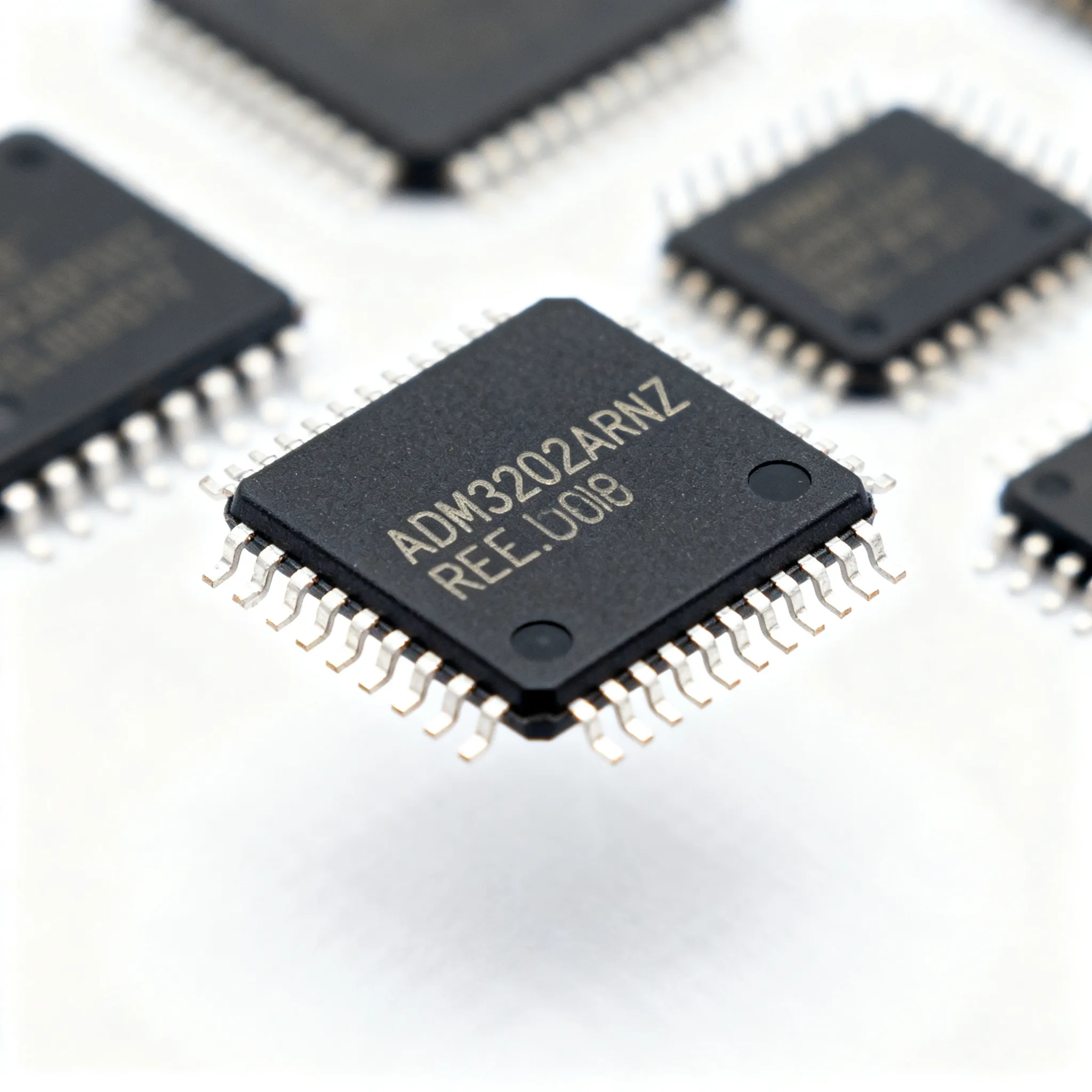
If you've been sourcing RS-232 transceivers over the past 18 months, you've learned that availability isn't something you can take for granted. The ADM3202ARNZ-REEL — a 3.3V, dual-channel RS-232 line driver/receiver in a 16-lead SOIC_N package — has remained one of the more consistently available parts from Analog Devices, but that doesn't mean engineers can afford to get complacent. Distributor stock levels at DigiKey show active replenishment, yet the part sits in a category where demand spikes can outstrip regional buffer stock within weeks. The ADM3202 family shares a common silicon die with the ADM3222 and ADM1385, meaning fab allocation decisions affect multiple SKUs simultaneously — a dynamic that procurement teams should factor into their reorder planning.
But here's the problem that catches even experienced engineers off guard: the PCB layout itself. A recent supply-chain advisory from ODG Electronics flagged a specific failure mode tied to trace width on the RS-232 output lines. The warning is worth quoting directly: "Ensure that the trace width is suitable for the current requirements to prevent overheating or signal degradation." This isn't boilerplate. RS-232 drivers push ±5.5V swings after the internal charge pump doubles the 3.3V rail. If your trace is too narrow on the driver output — especially on the V+ and V– charge pump pins — the increased current density can cause localized heating, degrade the output voltage swing, and ultimately violate the RS-232 minimum ±5V threshold at the connector. I've seen field returns where the root cause wasn't a defective transceiver but a 6-mil trace carrying charge pump current that should have been 12 mils wide.
What makes this trap particularly insidious is that the ADM3202ARNZ-REEL datasheet doesn't call out a minimum trace width explicitly. The guidance lives in the application notes and in the collective experience of engineers who've debugged marginal RS-232 links. The charge pump operates at approximately 250 kHz internally, and the peak currents during switching can be 10–15× the average DC load current. A trace that looks fine on a static IR drop analysis may sag unacceptably during the switching transient. The fix is straightforward: use at least 10-mil traces for the charge pump capacitor connections (C1+, C1–, C2+, C2–) and the V+ and V– pins, and keep those traces as short as physically possible. For the RS-232 driver outputs (T1OUT, T2OUT), 8-mil traces are generally adequate for the ~10 mA short-circuit current limit, but go wider if your board runs at elevated ambient temperatures.
Key Takeaway: The ADM3202ARNZ-REEL is available through authorized channels, but don't let a routine BOM entry lull you into skipping the layout review. The charge pump trace width issue is real, documented in field advisories, and entirely preventable with a few extra mils of copper.
Inside the ADM3202ARNZ-REEL: How a 3.3V, Dual-Channel RS-232 Transceiver Works Without Shutdown
The ADM3202ARNZ-REEL belongs to a family of high-speed RS-232/V.28 interface devices that operate from a single +3.3V power supply. Unlike its siblings — the ADM3222 and ADM1385 — the ADM3202 does not include a shutdown facility. That's a deliberate design choice: if your application needs to keep the RS-232 link alive at all times (think industrial HMIs, point-of-sale terminals, or medical monitoring equipment that maintains a debug serial console), the ADM3202 is the correct variant. The shutdown pin on the ADM3222 is useful for battery-powered portables, but it adds a control line and a potential failure mode. For always-on systems, eliminating the shutdown path simplifies firmware and removes one more thing that can go wrong during power sequencing.
At the core of the device is a capacitive charge pump voltage converter that generates ±5.5V rails from a single 3.3V input. The charge pump uses four external capacitors — typically 0.1 µF each — to double the supply voltage and then invert it. This architecture, documented in the official datasheet (Rev. E), eliminates the need for a separate negative supply rail, which simplifies power supply design and reduces BOM count. The trade-off is that the charge pump capacitors must be placed close to the IC and chosen with care — low-ESR ceramic capacitors with X7R dielectric are strongly recommended to maintain stable operation across the full –40°C to +85°C industrial temperature range.
The device supports data rates up to 460 kbps, which is well above the traditional 115.2 kbps ceiling for most RS-232 applications. This headroom matters when you're pushing firmware updates over a serial bootloader or streaming data from a high-sample-rate sensor. The receivers feature a 0.4V minimum input hysteresis, which provides solid noise immunity on long cable runs. ESD protection is rated at ±15 kV using the IEC 1000-4-2 air-gap discharge method on the RS-232 I/O pins, which is adequate for most commercial and light industrial environments.
The table below summarizes the key parameters you'll need when evaluating the ADM3202ARNZ-REEL against your design requirements:
| Parameter | Value/Range | Unit/Notes |
|---|---|---|
| Supply Voltage (VCC) | 3.0 to 3.6 (3.3V nominal ±10%) | V — Single supply |
| Supply Current (No Load) | 3.0 (typical) | mA |
| Supply Current (Shutdown) | N/A — ADM3202 has no shutdown pin | — |
| Data Rate (Minimum) | 460 | kbps |
| RS-232 Driver Output Swing | ±5.5 (typical, 3 kΩ load) | V |
| Receiver Input Threshold | 0.8 min / 2.4 max (VIL / VIH) | V — TTL/CMOS compatible |
| Receiver Input Hysteresis | 0.4 (minimum) | V |
| ESD Protection (I/O Pins) | ±15 kV (air-gap, IEC 1000-4-2) | kV |
| Charge Pump Capacitors | 0.1 (recommended) | µF — X7R, low ESR |
| Operating Temperature Range | –40 to +85 | °C — Industrial |
| Package | 16-Lead SOIC_N (R-16) | 4.9 mm body width |
| RoHS Compliance | Yes (Z suffix = lead-free) | — |
One parameter that deserves extra attention is the supply voltage tolerance. The ADM3202ARNZ-REEL is designed for a 3.3V rail, period. The ±10% window (3.0V to 3.6V) is tighter than many engineers expect. If your board has a 3.3V LDO that droops to 2.8V under heavy load, the charge pump may not generate a compliant RS-232 output level. The ADM3202 does not have undervoltage lockout, so it will attempt to operate — and the first symptom is usually intermittent communication failures that are maddening to debug. Always verify your 3.3V rail under worst-case load before signing off on the schematic.
For a complete understanding of the device, download the datasheet directly from LCSC or the Analog Devices product page. Both sources provide the full electrical characteristics, timing diagrams, and application circuit examples.
Decoding ADM3202 Suffixes: REEL, REEL7, and the Lead-Free Z That Matter for Your BOM
If you've ever stared at a BOM line item and wondered whether the difference between ADM3202ARNZ-REEL and ADM3202ARNZ-REEL7 actually matters for your assembly run, you're not alone. The suffixes encode packaging and reel quantity information that directly impacts your pick-and-place setup, your inventory planning, and — in the case of the "Z" — your regulatory compliance. Getting the suffix wrong won't change the silicon, but it can cause a line stoppage if your CM expects a 13-inch reel and receives a 7-inch one, or vice versa.
Let's break down the ordering code: ADM3202 is the base part number. AR indicates the SOIC_N (R-16) package. N denotes the industrial temperature range (–40°C to +85°C). Z is the Pb-free/RoHS-compliant designator. REEL means 2,500 units on a 13-inch reel with the standard orientation. REEL7 means 1,000 units on a 7-inch reel. The physical IC is identical; the difference is purely logistical. For high-volume production, REEL is the preferred choice because it minimizes reel changes on the SMT line. For prototyping, NPI builds, or low-volume production, REEL7 may be more practical because you're not tying up capital in 2,500 units.
The "Z" suffix deserves particular attention. The non-Z variant (ADM3202ARN) is not RoHS-compliant and may contain lead. If you're shipping to the EU, UK, China, or any market with RoHS-equivalent regulations, the "Z" is mandatory. Some distributors still carry non-Z inventory, and an inexperienced buyer might select the cheaper option without realizing the compliance risk. The cost difference is negligible in production volumes, but the compliance liability is enormous.
The table below compares the primary variants and a relevant alternative with enhanced ESD protection:
| Comparison Metric | ADM3202ARNZ-REEL | ADM3202ARNZ-REEL7 | ADM3202ARN (Non-Z) | ADM3232EARNZ (Enhanced ESD) |
|---|---|---|---|---|
| RoHS / Pb-Free | Yes (Z suffix) | Yes (Z suffix) | No — contains lead | Yes (Z suffix) |
| Reel Quantity | 2,500 units | 1,000 units | 2,500 units (typical) | Varies by ordering code |
| Reel Size | 13-inch | 7-inch | 13-inch | 13-inch / 7-inch options |
| Package | 16-SOIC_N (R-16) | 16-SOIC_N (R-16) | 16-SOIC_N (R-16) | 16-SOIC_N (R-16) |
| ESD — IEC Air Gap | ±15 kV | ±15 kV | ±15 kV | ±15 kV (enhanced) |
| ESD — IEC Contact | Not specified | Not specified | Not specified | ±15 kV |
| ESD — HBM | Not specified | Not specified | Not specified | ±8 kV |
| Shutdown Pin | No | No | No | No |
| Supply Voltage | 3.3V ±10% | 3.3V ±10% | 3.3V ±10% | 3.3V ±10% |
| Active Production | Yes | Yes | Limited / Phasing Out | Yes |
The ADM3232EARNZ, detailed in a comparison by Ovaga Technologies, is worth considering if your application faces frequent cable plug/unplug cycles or operates in an electrically noisy environment. The enhanced contact discharge rating (±15 kV vs. unspecified on the ADM3202) provides an additional margin of protection. However, the ADM3232EARNZ typically commands a small price premium, so the decision comes down to whether your application's ESD exposure justifies the extra cost. For a fixed internal connection inside an enclosure, the ADM3202ARNZ-REEL is almost always sufficient. For a connector exposed to user handling — a debug port on the back of a rack-mount unit, for example — the enhanced protection of the ADM3232EARNZ is cheap insurance.
Another comparison worth noting is between the ADM3202ARN and the ADM3202ARNZ-REEL7, as analyzed by Ovaga. The silicon is the same, but the RoHS compliance difference is a hard gate for any design shipping to regulated markets. The ETEI Electronic comparison between REEL7 and REEL variants confirms that the distinction is purely in reel geometry and quantity — the device on the tape is identical. For procurement, this means you can switch between REEL and REEL7 without requalification, as long as your assembly house can handle both reel sizes.
Laying Out the ADM3202ARNZ-REEL: Charge Pump Capacitors, Trace Width Rules, and Sourcing to Avoid Counterfeits
A well-designed schematic with the ADM3202ARNZ-REEL can still fail in the field if the layout ignores the charge pump's switching dynamics. The four external capacitors — C1, C2, C3, and C4 — are not bypass capacitors in the conventional sense. They are energy transfer elements in a switched-capacitor voltage converter operating at roughly 250 kHz internally. Every millimeter of trace between the capacitor and the IC pin adds inductance that degrades the charge pump's efficiency, increases ripple on the V+ and V– rails, and can cause the RS-232 output swing to collapse under load.
Here's a practical layout checklist that goes beyond the datasheet's schematic:
- Place C1, C2, C3, and C4 within 5 mm of the IC pins. The C1+ and C1– pins (pins 1 and 3) connect to the flying capacitor C1. The C2+ and C2– pins (pins 4 and 5) connect to C2. C3 connects between V+ (pin 2) and GND. C4 connects between V– (pin 6) and GND. If any of these capacitors is more than 10 mm from its pins, you're inviting trouble.
- Use 10-mil minimum trace width for all charge pump connections. As flagged in the ODG Electronics advisory, trace width is not a cosmetic choice here. The peak currents during charge pump switching are significantly higher than the DC load current. Narrow traces increase resistance, which reduces the voltage delivered to the storage capacitors and increases ripple.
- Route V+ and V– traces as power rails, not signals. These nets carry the ±5.5V supply for the RS-232 drivers. Treat them with the same care you'd give to a switching regulator's output. Use 12–15 mil traces, and consider a small (1 µF) ceramic bypass capacitor at the V+ and V– pins in addition to the 0.1 µF charge pump capacitors if your layout forces longer trace lengths.
- Keep the ground plane solid under the charge pump section. Don't split the ground plane or route digital signals through the charge pump area. The switching currents in the capacitors create magnetic fields that can couple into nearby high-impedance nodes.
- Place the 0.1 µF VCC bypass capacitor as close to pin 16 as possible. This is standard practice for any IC, but it's doubly important here because the charge pump draws pulsed current from VCC.
- Route RS-232 output traces (T1OUT, T2OUT) at 8–10 mils minimum. The short-circuit current limit is approximately 10 mA per driver, which isn't extreme, but the voltage swing is ±5.5V. Wider traces reduce the IR drop to the connector, ensuring the signal at the far end of the cable meets the ±5V RS-232 threshold.
Tip: If you're using a 2-layer board, run the charge pump capacitors on the top layer with direct connections to the IC pins. Don't drop vias into the charge pump loop unless absolutely necessary — each via adds roughly 0.5–1 nH of inductance, and at 250 kHz switching frequency, even a few nanohenries matter.
The capacitor selection itself is relatively straightforward, but the dielectric and voltage rating choices have consequences:
| Capacitor | Recommended Value | Dielectric | Voltage Rating | Selection Rationale |
|---|---|---|---|---|
| C1 (Flying Cap 1) | 0.1 µF | X7R | ≥16V | Sees VCC + V+ voltage swing; 16V provides margin |
| C2 (Flying Cap 2) | 0.1 µF | X7R | ≥16V | Same as C1 — switched in the inverter stage |
| C3 (V+ Storage) | 0.1 µF | X7R | ≥16V | Stores the doubled voltage (~6.6V at no load) |
| C4 (V– Storage) | 0.1 µF | X7R | ≥16V | Stores the inverted voltage (~–6.6V at no load) |
| VCC Bypass | 0.1 µF | X7R | ≥10V | Standard supply decoupling; 10V sufficient for 3.3V rail |
X7R is specified because it maintains capacitance within ±15% across the –40°C to +85°C range. Y5V or Z5U dielectrics can lose 60–80% of their capacitance at temperature extremes, which can cause the charge pump to lose regulation. Don't save a fraction of a cent on capacitors and create an intermittent field failure that costs thousands to debug.
On the sourcing side, the ADM3202ARNZ-REEL is available through authorized distributors including DigiKey and LCSC. Third-party sources like Cytech Systems and ODG Electronics also list the part, but when buying from non-authorized channels, you should verify authenticity through ADI's counterfeit detection resources. Counterfeit RS-232 transceivers are a known problem in the secondary market — they may work on the bench but fail in the field due to substandard ESD protection or charge pump performance. The cost of a single field return dwarfs any per-unit savings from grey-market sourcing.
ADM3202ARNZ-REEL: Questions Engineers and Buyers Ask Before Finalizing the BOM
After two decades of specifying RS-232 interface ICs, I've noticed that the same questions come up repeatedly — whether from a junior engineer doing their first serial port design or a seasoned buyer trying to reconcile BOM variants. Here are the answers to the six most common questions about the ADM3202ARNZ-REEL.
Q: What's the difference between ADM3202ARNZ-REEL and ADM3202ARNZ-REEL7?
The only difference is the reel quantity and orientation: REEL is typically 2,500 units on a 13-inch reel, while REEL7 is 1,000 units on a 7-inch reel. The physical device is identical — same silicon, same package, same test program. If your assembly line can handle both reel sizes, you can use either interchangeably without any requalification. For high-volume production, REEL is more cost-effective because it reduces reel-change downtime. For prototyping or low-volume builds, REEL7 is often more practical. LCSC stocks the ADM3202ARNZ-REEL7 variant, which is a good option if you need smaller quantities.
Q: Can I power the ADM3202ARNZ-REEL from a 5V supply?
No. The ADM3202ARNZ-REEL is designed for a single 3.3V supply with a ±10% tolerance (3.0V to 3.6V). Applying 5V will exceed the absolute maximum rating and can permanently damage the device. More subtly, even if the device survives, the charge pump is optimized for 3.3V input — a 5V input would generate RS-232 output levels that exceed the ±25V absolute maximum rating of the RS-232 standard, potentially damaging the receiver on the other end of the cable. For 5V applications, consider the ADM202 family, which is designed for 5V operation with a similar charge pump architecture. The ADM3202 product page clearly lists the supply voltage range — don't assume RS-232 transceivers are supply-voltage agnostic.
Q: Does the ADM3202ARNZ-REEL have built-in ESD protection?
Yes, it meets ±15 kV IEC 1000-4-2 air-gap discharge on the RS-232 I/O pins. However, this rating applies to air-gap discharge only. The device does not specify IEC contact discharge or HBM (Human Body Model) ratings. If your application involves frequent cable mating/unmating or exposed connectors, consider the ADM3232EARNZ, which offers enhanced ±15 kV contact discharge and ±8 kV HBM protection. The Ovaga comparison between the ADM3232EARNZ and ADM3202ARNZ-REEL7 breaks down the ESD specifications in detail. For a fixed internal connection inside a sealed enclosure, the ADM3202's protection is typically sufficient. For a user-accessible port, the enhanced protection is worth the incremental cost.
Q: What are the recommended charge pump capacitor values?
The datasheet recommends 0.1 µF capacitors for C1, C2, C3, and C4. Use low-ESR ceramic capacitors with X7R dielectric to ensure stable charge pump operation across the full –40°C to +85°C temperature range. The voltage rating should be at least 16V to provide margin above the peak charge pump voltages. While the datasheet specifies 0.1 µF, I've seen designs successfully use 0.22 µF or 0.47 µF capacitors when the layout forces longer trace lengths — the extra capacitance helps compensate for the increased inductance. However, larger capacitors increase the inrush current at startup, which can cause a brief dip on the 3.3V rail. If you deviate from the 0.1 µF recommendation, test the power-up sequence thoroughly. The datasheet from LCSC includes the recommended application circuit.
Q: Is the ADM3202ARNZ-REEL still in active production?
Yes, Analog Devices continues to manufacture the ADM3202ARNZ-REEL. The device is listed as active on the ADI product page, and authorized distributors maintain active stock. The ADM3202 family has been in production for over 15 years and shows no signs of obsolescence. However, the non-RoHS ADM3202ARN variant is being phased out in favor of the lead-free Z-suffix versions. If your design still specifies the non-Z part, now is the time to transition. For the latest lifecycle status, verify with the manufacturer or request a quote through authorized channels.
Q: How do I verify that I'm buying genuine ADM3202ARNZ-REEL parts?
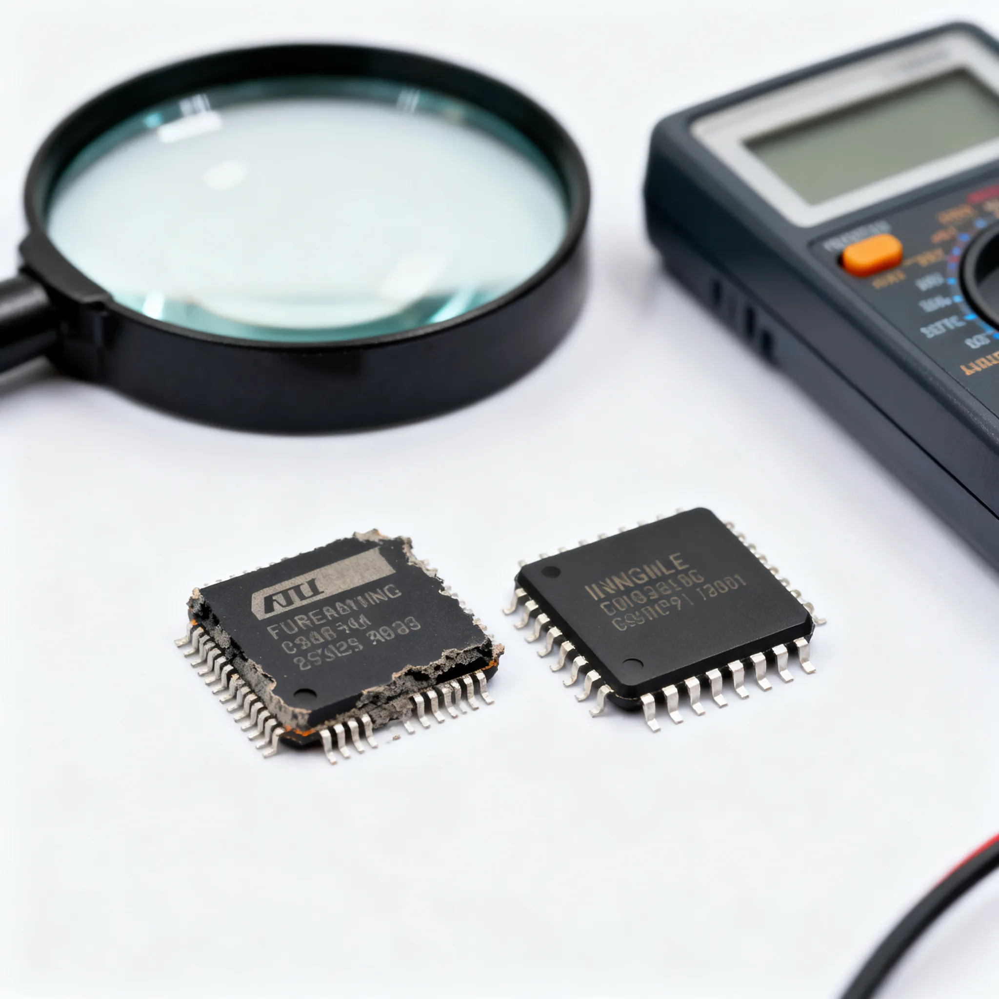
Purchase from ADI's authorized distributors — DigiKey, Mouser, and other franchised partners listed on the Analog Devices website. These distributors source directly from ADI and provide full traceability. If you're sourcing from third-party platforms like Cytech Systems or ODG Electronics, cross-check the supplier against ADI's authorized distributor list. Analog Devices provides counterfeit detection tools and resources on their website. Visual inspection can catch some counterfeits — look for inconsistent laser marking, rough package edges, or pins that don't align with the SOIC-16 footprint. But the most reliable defense is buying from authorized sources. A counterfeit RS-232 transceiver may work initially but fail due to substandard ESD protection or a charge pump that can't deliver the rated output swing. The cost of a field failure — including diagnosis, replacement, and reputational damage — far exceeds any savings from grey-market sourcing.
References & Further Reading
- ADM3202 Product Page — Analog Devices: Official product page with datasheet downloads, application notes, and ordering information.
- ADM3202/ADM3222/ADM1385 Datasheet Rev. E — Analog Devices: Complete electrical specifications, timing diagrams, and application circuits.
- ADM3202ARNZ-REEL