BSS138 Datasheet and Pinout: Specs for Design and Sourcing
BSS138 datasheet essentials, pinout overview, key specs, and design/sourcing checks for engineers and buyers. Request a quote on IC-Online.
Why BSS138 Remains the Go-To Logic-Level FET in 2024: Datasheet Revisions and Multi-Supplier Signals
The BSS138 is far from a legacy component gathering dust in outdated BOMs. A fresh look at manufacturer activity reveals a thriving multi-source ecosystem that continues to invest in this tiny SOT‑23 N‑channel MOSFET. Diodes Incorporated issued a revised datasheet (DS30144 Rev. 25, June 2024) with refined characterisation curves and footprint guidance [source]. Meanwhile PANJIT maintains active listings on high‑volume distribution platforms like LCSC, complete with downloadable datasheets [source]. Onsemi’s parametric summaries consistently reinforce the core ratings — 50 V drain‑source voltage and 220 mA continuous drain current — that have made the part a staple for level shifting, load switching, and signal inversion [source]. Together, these signals confirm that the BSS138 is anything but obsolete; it is a living product supported by multiple qualified suppliers.
For design engineers and procurement professionals, the implication is clear: you can specify the BSS138 with confidence, but you must remain vigilant about pinout references and package variants. With each supplier using slightly different marking codes and internal bonding, a footprint that works for one manufacturer’s BSS138 may need re‑verification when switching to another. Staying aligned with the latest datasheets — not a cached PDF from a decade ago — is the only way to avoid layout surprises and electrical margin errors.
Reading the BSS138 Pinout and Absolute Maximums to Prevent Design Margin Errors
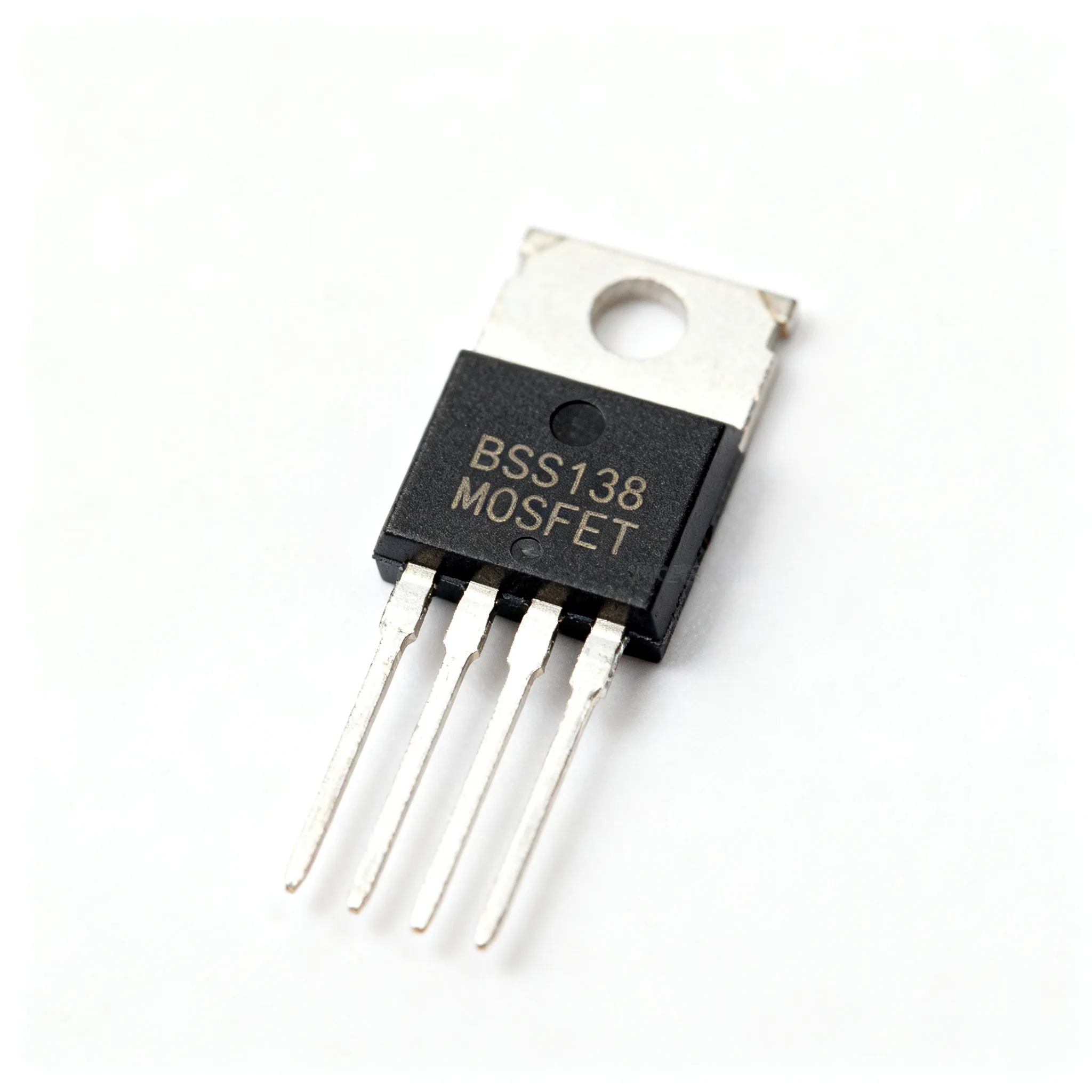
The standard SOT‑23 pinout of the BSS138 is deceptively simple: Gate is pin 1, Source is pin 2, and Drain is pin 3 [source]. This arrangement is consistent across all major manufacturers, yet it is still surprisingly easy to transpose Drain and Source in a rush layout. Doing so turns a low‑side switch into a forward‑biased diode, potentially destroying the MOSFET or the circuit it was meant to protect. A quick‑look table of absolute maximum ratings — drawn from Onsemi’s and Fairchild’s official documents [source][source] — helps establish safe operating boundaries before any traces are routed.
| Parameter | Symbol | Rating | Unit | Conditions / Notes |
|---|---|---|---|---|
| Drain‑Source Voltage | VDSS | 50 | V | TA=25 °C |
| Gate‑Source Voltage | VGSS | ±20 | V | DC, across full temperature range |
| Continuous Drain Current | ID | 220 | mA | TA=25 °C; derate above 25 °C per datasheet |
| Pulsed Drain Current | IDM | 880 | mA | Pulse width ≤ 300 µs, duty cycle ≤ 2% |
| Power Dissipation | PD | 350 | mW | SOT‑23, TA=25 °C; linearly derate above 25 °C |
| Operating Junction Temperature | TJ | ‑55 to +150 | °C | Storage range identical |
Beyond the brick‑wall limits, the electrical characteristics that define real‑world performance must be weighed carefully. The BSS138 is prized for its low gate threshold voltage — typically 0.5 V to 1.5 V — which makes it a natural fit for 1.8 V and 3.3 V logic [source]. On‑resistance, however, varies strongly with gate drive: expect a maximum RDS(on) of 3.5 Ω at VGS=10 V, rising to 6.0 Ω at VGS=4.5 V. Input capacitance sits at a modest 40 pF, and total gate charge hovers around 2 nC, enabling fast switching with transition times (ton+toff) frequently below 25 ns [source]. For low‑frequency applications these numbers look comfortable, but designers driving a gate directly from a weak microcontroller GPIO must check the transfer curve to ensure the drain current at the applied VGS meets the load requirement.
Tip: Always over‑voltage protect the gate. The fragile gate oxide of the BSS138 will rupture above 20 V. Even a small ESD event or a ringing 3.3 V rail can punch through if no external zener clamp is present. Add a 10 V–15 V zener from Gate to Source and a series gate resistor of 100 Ω–1 kΩ to keep transients within the safe window.
BSS138 vs. 2N7002: Choosing the Right Small-Signal MOSFET When Every Nanoamp and Ohm Counts
The BSS138 and the 2N7002 occupy the same compact SOT‑23 real estate, but their electrical personalities diverge in ways that directly affect BOM cost and circuit reliability. The 2N7002 is often cited as a lower‑cost alternative worth evaluating when gate drive voltage is generous [source]. However, a side‑by‑side comparison reveals that the BSS138 holds a distinct advantage in threshold voltage, RDS(on) at low VGS, and switching speed — factors that can dictate whether a design needs an extra level‑shifter stage.
| Comparison Metric | BSS138 (N‑Channel SOT‑23) | 2N7002 (N‑Channel SOT‑23) | Selection Criteria & Failure Boundary |
|---|---|---|---|
| Typical VGS(th) range | 0.5 V – 1.5 V | 1.0 V – 2.5 V | BSS138 turns on with 1.8 V logic; 2N7002 may not fully enhance at 3.3 V, risking higher conduction loss. |
| RDS(on) at VGS=4.5 V | ≤ 6.0 Ω | ≤ 7.5 Ω (often ~5 Ω typical) | Similar at strong gate drive; BSS138 offers slightly lower worst‑case for equal dissipation. |
| Input capacitance Ciss | ~40 pF | ~50 pF | BSS138 yields faster switching edges; meaningful for PWM above 500 kHz. |
| Continuous ID at 25 °C | 220 mA | 200–300 mA (varies by mfr.) | Both sufficient for logic‑level loads; verify derating at elevated ambient. |
| Price indication (reel qty 3k+) | $0.015–$0.05 [source] | $0.010–$0.04 | 2N7002 can be 10–30% less expensive; evaluate if threshold margin permits. |
| Typical lead time | In stock to 8 weeks (multi‑source) | In stock to 12 weeks | Both allocation‑sensitive during surges; confirm via authorised distributor. |
The BSS138 justifies its slightly higher price in any circuit where the gate is driven by a low‑voltage GPIO or where the MOSFET must switch cleanly at sub‑100 mA currents without a large gate‑drive boost. The 2N7002 becomes an attractive candidate when the gate is firmly switched with 5 V or higher, and when the budget for high‑volume consumer products demands every fraction of a cent shaved from the BOM. Still, managers should verify the actual RDS(on) distribution of the chosen 2N7002 manufacturer — some legacy processes yield parts with thresholds approaching 2.5 V, dangerously close to the output swing of a 3.3 V microcontroller at elevated temperature. Always bench‑test the worst‑case lot before committing a production board.
Sourcing BSS138 Without Falling into Counterfeit, Long Lead‑Time, or Pinout Traps
A multi‑source ecosystem — Onsemi, Diodes Incorporated, PANJIT, and the former Fairchild lines now under Onsemi — works in the buyer’s favour, but it also opens the door to subtle discrepancies in marking and packaging. Procurement teams should treat the BSS138 as a part where visual inspection and parametric verification are not optional. The top‑side marking differs by supplier: Onsemi’s BSS138LT1G uses “1J”, while Diodes’ variant may show “BSS138” or “K38” [source]. If a reel arrives with a marking that mismatches the manufacturer‑specific datasheet, that batch demands scrutiny.
Authorised distributor aggregators such as Octopart provide a live window into availability and pricing across Onsemi and Diodes channels [source]. The practice of source‑controlled procurement reduces the risk of remarked or off‑spec clones. Yet even from an authorised source, design teams should enforce a quick incoming‑inspection routine: measure RDS(on) at VGS=4.5 V on a sample of 10–20 units. If any unit exceeds 6 Ω, reject the lot. The same sample can be checked for gate leakage at 10 V; anything above 100 nA points to oxide damage.
Key procurement checklist for the BSS138:
| Verification Step | What to Require | Red Flag |
|---|---|---|
| Manufacturer datasheet alignment | Current revision obtained directly from manufacturer’s website [source][source] | Datasheet dated before 2015 lacking Pb‑free or MSL notes |
| Top marking verification | Marking code confirmed against supplier’s datasheet (e.g., “1J” for Onsemi BSS138LT1G) | Lasered marking with irregular font; date code inconsistent with lot traceability |
| RDS(on) sample test | ≤ 6 Ω at VGS=4.5 V, ID=100 mA, Tamb=25 °C | Any unit above 6 Ω; batch average significantly higher than 3.5 Ω |
| Gate leakage | IGSS < 100 nA at VGS=10 V | Leakage > 1 µA indicates oxide punch‑through |
| Package integrity | Standard SOT‑23, pin 1 (Gate) clearly identified; footprint matches IPC‑7351 SOT‑23 reference | Reversed orientation on tape; pin 1 dot missing |
From a design‑review standpoint, the PCB footprint for the BSS138 must strictly follow pin 1 assignment with a clear silkscreen indicator. A gate‑source zener and a 100 Ω resistor cost less than a penny but prevent field failures caused by ESD or over‑voltage ringing. Verify moisture sensitivity level (MSL) ratings — typically MSL1 — and ensure the chosen reel packaging meets your assembly house’s baking requirements if parts have been stored beyond floor‑life limits.
BSS138 Design and Procurement FAQs: Questions Senior Engineers and Buyers Actually Ask
Q: Can I safely drive the BSS138 with a 3.3 V microcontroller GPIO?
Yes, the typical threshold voltage of 0.5–1.5 V ensures that a 3.3 V logic high will enhance the channel. Datasheets guarantee RDS(on) at VGS=4.5 V, but with a 3.3 V gate the device will still fully turn on for drain currents below approximately 100 mA. Always check the transfer curve (Figure 2 in the Onsemi datasheet [source]) to confirm that the current at VGS=3.3 V meets your load requirement. In level‑shifting applications, a 1.8 V to 3.3 V conversion operates far inside the safe region.
Q: What is the difference between BSS138, BSS138L, and BSS138DW?
The BSS138 is the standard single N‑channel MOSFET in an SOT‑23 package. BSS138L is a very‑low‑threshold variant with VGS(th) often below 0.6 V, optimised for 1.2 V logic. BSS138DW is a dual‑die device housed in an SOT‑363 package containing two independent BSS138 channels. Always match the exact part number to the manufacturer’s latest datasheet; a footprint designed for the single SOT‑23 BSS138 will not fit the dual package.
Q: How do I identify legitimate BSS138 parts versus remarked or off‑spec clones?
Verify the top marking against the manufacturer’s datasheet — Onsemi uses “1J” for the BSS138LT1G, while Diodes may print “BSS138” or “K38”. Cross‑check the lot code with an authorised distributor and request a sample batch for a quick parametric test: measure RDS(on) at VGS=4.5 V with a current source of 100 mA. If any device reads higher than 6 Ω, reject the batch. Rely on authorised channels visible on Octopart [source] and avoid unverified spot‑market brokers.
Q: Is the Fairchild BSS138 datasheet from 2005 still valid for current Onsemi production?
Yes, Onsemi inherited the Fairchild portfolio and the 2005 datasheet [source] still provides final specifications. However, Onsemi has since released its own revision ([source]). Always use the manufacturer‑specific current datasheet for your purchased part because thermal performance, ESD ratings, and parametric distributions can shift over decades of process refinement.
Q: What are typical lead times and price breaks for BSS138 from major distributors?
Lead times for the standard SOT‑23 BSS138 vary by manufacturer but are commonly in stock to 8 weeks under normal demand. Prices in reel quantities (3,000–10,000 units) fall in the $0.015–$0.05 range. Aggregate inventory presented on Octopart [source] is a useful starting point, but procurement should confirm allocation‑backed lead time directly with the supplier. Both Onsemi and Diodes channels are historically robust, yet any single‑source arrangement can become allocation‑sensitive during unexpected demand spikes — verify multi‑supplier qualification to mitigate risk.
Q: Can I use the BSS138 for high‑speed PWM above 500 kHz?
The BSS138’s low total gate charge (~2 nC) and fast switching characteristics (ton+toff <25 ns) make it suitable for PWM frequencies up to about 1 MHz [source]. However, gate drive strength becomes critical at those speeds; a high‑impedance GPIO output will cause excessive switching losses. Use a dedicated gate driver or a push‑pull buffer to maintain clean edges. For sustained high‑current PWM near the 220 mA limit, verify the safe operating area (SOA) curve and account for RDS(on) increase with junction temperature — derating may be necessary above 85 °C ambient.
References & Further Reading
- Diodes BSS138 Datasheet, DS30144 Rev. 25, June 2024
- PANJIT BSS138 Datasheet, LCSC Electronics
- BSS138 Onsemi Overview, All About Circuits
- BSS138 MOSFET Pinout, Datasheet, Equivalent – Components101
- Onsemi BSS138 Data Sheet
- Fairchild BSS138 Datasheet (2005) via SparkFun
- BSS138 Datasheet: Specifications, Pinout, and Application Notes – TechDiagrammer
- BSS138 N-Channel Transistor: Pinout, Datasheet and Equivalent – Utmel
- BSS138 onsemi – Distributors, Price Comparison, and Datasheets – Octopart
Design and procurement decisions around the BSS138 ultimately hinge on having the right datasheet, a validated footprint, and a trusted supply chain. When you’re ready to secure production quantities or need to verify current allocation, upload your BOM or request a quote through IC-Online. Our team supports mixed BOMs with flexible MOQ and can help you source authentic BSS138 parts from authorised channels, keeping your schedule and budget on track.