

CM400DY-24A Datasheet and Pinout: Specs for Design and Sourcing
CM400DY-24A datasheet essentials, pinout overview, key specs, and design/sourcing checks for engineers and buyers. Request a quote on IC-Online.
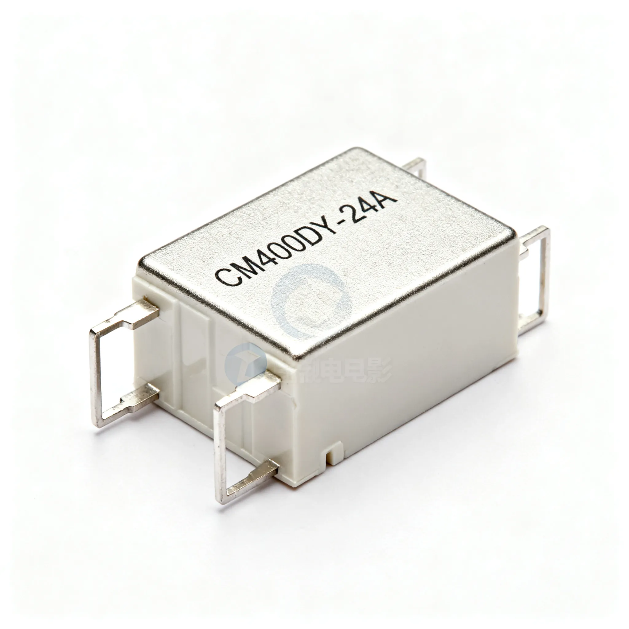
Why the CM400DY-24A Remains a Go-To Module in High-Power Switching—and the Sourcing Hurdles You’ll Face
The CM400DY-24A dual IGBT module from Mitsubishi Electric has been a workhorse in industrial motor drives, uninterruptible power supplies, and welding inverters for over a decade. Even as newer A-series and higher-density generations emerge, service depots and retrofit projects still rely on this 1200 V / 400 A half-bridge because it delivers predictable switching performance, a rugged NPT (non-punch-through) IGBT structure, and a well-documented mechanical footprint. Yet anyone who has tried to source the CM400DY-24A in the last two years knows the real friction: fragmented documentation, inconsistent date-code labeling, and the constant risk of relabeled pulls being sold as “new”.
The datasheet landscape alone tells the story. A compact 5‑page, 47 Kbyte PDF circulates on Alldatasheet (source) and on DigChip (source), while a slightly larger 103 Kbyte version also appears under the same part number (103 Kb datasheet). Both are genuine Mitsubishi documents, but the short form omits some switching-energy curves and derating details that engineers need for borderline thermal designs. Meanwhile, distributors such as IC Components list the CM400DY-24A and host a scanned copy of the 5‑page datasheet (source), but their listing does not guarantee real-time inventory—it simply confirms that the module is still traded on the open market.
Mitsubishi’s own product page (source) classifies the CM400DY-24A as a legacy A-series module, which means it is not recommended for new designs, though it remains available through distribution channels for maintenance and repair. That status injects a sourcing challenge: you are essentially buying from aftermarket or channel stock, and you must treat supply as allocation-sensitive. Before you specify or order the part, you need to ground every design decision in the authentic pinout and maximum ratings—and then verify that the modules you receive match the datasheet electrical characteristics and the mechanical drawing precisely.
Pinout, Internal Schematic, and the Numbers That Define the CM400DY-24A
The CM400DY-24A module houses a half‑bridge formed by two N‑channel IGBTs and two anti‑parallel free‑wheeling diodes. The internal connection ties the emitter of the upper IGBT to the collector of the lower IGBT, which is why the middle power terminal is labeled C2E1—it serves as the collector of the lower device and the emitter of the upper device simultaneously. The external terminals are:
- C1 – Collector of the upper IGBT (positive DC bus)
- C2E1 – Phase output / mid‑point (emitter of upper IGBT, collector of lower IGBT)
- E2 – Emitter of the lower IGBT (negative DC bus)
- G1 – Gate of the upper IGBT
- G2 – Gate of the lower IGBT
- Auxiliary emitter terminals (E1 sense, E2 sense) for kelvin gate‑drive connection
The terminal arrangement is clearly dimensioned in the mechanical drawing available in the Mouser‑hosted datasheet (source). That drawing also shows the mounting hole pattern, the location of the label tab (#110), and the overall envelope—critical for heatsink interface and bus-bar layout. Missing the sense‑emitter pins can lead to gate‑emitter overvoltage and premature failure, so the pinout is not simply “six bolts”; the small auxiliary terminals are integral to proper gate‑drive design.
The absolute maximum ratings, reproduced from the 103 Kbyte datasheet and the official Mitsubishi profile, define the safe operating boundaries. The table below collects the tier‑A parameters every engineer needs before designing a gate drive or thermal stack.
| Parameter | Value | Unit / Notes |
|---|---|---|
| Collector‑Emitter Voltage (VCES) | 1200 | V, Tj = 25 °C |
| Gate‑Emitter Voltage (VGES) | ±20 | V |
| Collector Current, DC (IC) | 400 | A, Tc = 80 °C |
| Collector Current, Pulse (ICP) | 800 | A, 1 ms |
| Collector Power Dissipation (Pc) | 2710 | W |
| Junction Temperature (Tj) | −40 to +150 | °C |
| Storage Temperature (Tstg) | −40 to +125 | °C |
| Isolation Voltage (Visol) | 2500 | V AC, 1 min, 60 Hz |
| Mounting Torque, Power Terminals | 3.5 | N·m |
| Mounting Torque, Module to Heatsink | 3.5 | N·m |
| Weight | 350 | g (approx.) |
Tip: The 400 A rating is given at Tc = 80 °C. In a real inverter, the case temperature often sits between 85 °C and 100 °C under heavy load, so you must derate IC using the safe operating area curves in the full datasheet. The 103 Kbyte version (link) includes the forward safe operating area (FSOA) and reverse bias safe operating area (RBSOA) plots that are missing from the 47 Kbyte abstract.
CM400DY-24A vs. Alternative 1200V/400A Dual Modules: What to Compare Before You Substitute
When a CM400DY-24A is flagged as long‑lead or requires allocation confirmation, engineers often look for a 1200 V / 400 A dual module that fits the same bus‑bar layout and heatsink cutout. The Infineon FF400R12KE3 and SEMIKRON SKM400GB12T4 are the two most frequently cited evaluation candidates, and Mitsubishi’s own A‑series successors (such as the NFH‑type modules) appear in Octopart price comparisons (source). However, a parameter‑by‑parameter comparison reveals why a “drop‑in” swap is rarely straightforward.
The table below lines up the CM400DY-24A against the two common alternatives. All values are drawn from manufacturer datasheets and should be verified with the latest revision before final selection.
| Parameter | CM400DY-24A | FF400R12KE3 | SKM400GB12T4 | Selection / Verification Note |
|---|---|---|---|---|
| VCES (V) | 1200 | 1200 | 1200 | All match; verify VCES headroom with your DC‑link voltage. |
| IC (A) at Tc = 80 °C | 400 | 400 | 400 | Same base rating; derating curves differ slightly. |
| VCE(sat) typ. (V) | 1.7 | 1.7 | 1.8 | SKM400GB12T4 has slightly higher conduction loss; check thermal budget. |
| Rth(j‑c) IGBT per switch (K/W) | 0.08 | 0.08 | 0.09 | SEMIKRON’s higher thermal resistance may require a larger heatsink. |
| Package outline | Mitsubishi “CM” dual, 6‑bolt | Infineon 62 mm C‑series | SEMITRANS 3 | Footprint and bus‑bar holes are not identical; mechanical rework is almost certain. |
| Gate drive voltage | ±20 V | ±20 V | ±20 V | Gate‑drive interface is compatible, but gate‑charge and Miller plateau differ. |
| Internal free‑wheeling diode | Yes | Yes | Yes | Reverse recovery charge (Qrr) varies; verify snubber and EMI filter impact. |
Start your substitute search on the Alldatasheet multi‑result page for the base string “CM400DY-24” (source), which pulls up the original Mitsubishi documents and sometimes the NF variant. Use Octopart (source) to compare current distributor‑quoted lead‑time signals (not numeric lead times, but “in stock” vs. “call for availability” flags). The Mouser‑hosted mechanical drawing (source) is your reference for the original CM400DY-24A package: any candidate that deviates by more than 0.5 mm in the mounting hole pattern will force a heatsink redesign.
Designing In and Sourcing the CM400DY-24A: Gate Drive, Heat Management, and Avoiding Counterfeits
Because the CM400DY-24A is a legacy module, your design and procurement process must be built around the reality that the documentation is fixed but the supply chain is fluid. The official Mitsubishi product profile (source) remains the authoritative source for electrical characteristics, and the 103 Kbyte datasheet (source) provides the switching energy curves you need to size the gate resistor and calculate dead time.
Gate drive best practices:
- Drive the gates with a bipolar supply that clamps the gate‑emitter voltage to ±20 V. The datasheet switching characteristics (turn‑on time ton, turn‑off time toff) are specified with RG = 0.5 Ω. Start with a gate resistor between 0.5 Ω and 2 Ω and adjust based on measured dv/dt and the collector‑emitter ringing.
- Use the auxiliary emitter terminals (E1 sense, E2 sense) for the gate‑drive return path—never route the gate‑return through the power emitter bolt. That Kelvin connection avoids the di/dt‑induced voltage drop that can lift the emitter potential and cause spurious turn‑on.
- Apply the mounting torque of 3.5 N·m exactly as specified in the Mouser datasheet (source). Over‑torque can crack the ceramic substrate; under‑torque increases thermal resistance.
Procurement and counterfeit avoidance:
IC Components lists the CM400DY-24A and has hosted a datasheet copy (source). While that signals market availability, it does not guarantee that every unit shipped is factory‑fresh. Modules that have been pulled from decommissioned equipment can be cleaned, relabeled, and sold as “new old stock.” To protect your production line, build a receiving inspection protocol that includes the checks in the table below and require that your supplier confirms current allocation-backed lead time and provides a certificate of conformance with a traceable date code.
| Check Item | Method / Equipment | Pass / Fail Criteria |
|---|---|---|
| Date code verification | Visual inspection of label TAB #110 (see Mouser datasheet); cross‑reference with DigChip (source) for format. | Code must be legible and match the manufacturer’s 4‑digit format; no evidence of over‑labeling. |
| VCE(sat) measurement at IC = 400 A | Curve tracer or dynamic test at 10 μs pulse, Tj ≈ 25 °C. | Typical 1.7 V; < 2.0 V under specified conditions. Higher values suggest bond‑wire degradation. |
| Free‑wheel diode forward voltage (VF) | IF = 400 A, short pulse. | Typical 1.5 V; any unit exceeding 1.8 V should be quarantined. |
| Gate threshold voltage (VGE(th)) | IC = 400 mA, VCE = VGE. | 4.0–6.5 V; an outlier indicates gate oxide damage. |
| Insulation resistance | 500 V DC between all terminals shorted and baseplate. | > 10 MΩ; lower values point to moisture ingress or ceramic crack. |
Use DigChip (source) to cross‑reference the part number against older date codes and alternative labeling formats that appear on surplus inventory. If a supplier’s lot includes modules with date codes spread over more than three years, ask for a lot‑specific test report before accepting the order.
CM400DY-24A: Questions Engineers and Buyers Frequently Ask
Q: What is the exact pinout of the CM400DY-24A?
The module has main power terminals C1, C2E1, and E2, plus gate terminals G1 and G2. The internal connection ties the emitter of the upper IGBT to the collector of the lower IGBT, forming a half‑bridge with free‑wheeling diodes across each device. The datasheet (Mouser link) includes a clear terminal arrangement diagram and the auxiliary emitter terminals for gate drive. Always use the sense‑emitter pins for the gate‑return path to avoid di/dt‑induced voltage drops on the power‑emitter path.
Q: Is the CM400DY-24A still in active production?
Mitsubishi lists it as a legacy A‑series module; it is not recommended for new designs. However, distributors like IC Components and surplus stock sources still carry it, making it available for maintenance and repair. Always verify date codes and traceability before purchasing—treat supply as allocation‑sensitive and confirm current availability via RFQ with your distributor.
Q: Can I replace a CM400DY-24A with a CM400DY-24NF?
No, the CM400DY-24NF is a different package (generally a larger form factor) and often has different internal connections and ratings. The CM400DY-24A is a dual module with a specific pinout; substitutes must match the mechanical footprint and electrical ratings. Check the datasheet comparisons on Alldatasheet or Octopart for verified alternatives and always verify the mechanical drawing against the Mouser‑hosted datasheet before considering any substitute.
Q: What gate resistor value should I use to drive the CM400DY-24A?
The optimal gate resistor depends on the desired switching speed and EMI limits. The datasheet’s switching characteristics (turn‑on/turn‑off times) are specified with a gate resistor of 0.5 Ω typical. Start with a value in the range of 0.5–2 Ω and adjust based on your gate drive voltage and measured dv/dt, ensuring the gate voltage does not exceed ±20 V. Use the 103 Kbyte datasheet’s switching energy curves to predict Eon and Eoff for your operating conditions.
Q: How do I read the date code from the CM400DY-24A label?
Mitsubishi modules typically use a four‑digit code (YYWW) or a serialised format. The label on the module (shown in the Mouser datasheet) includes a ‘LABEL TAB #110’ with markings. Cross‑reference the number with Mitsubishi’s date code appnote or contact a distributor to confirm the manufacturing week and year. Relabeled modules often show a fresh label over an older one—inspect under magnification.
Q: What are the most common failure modes in field returns?
Bond wire lift‑off due to thermal cycling, solder fatigue at the module‑to‑heatsink interface, and gate oxide degradation from overvoltage or static discharge are frequent. Testing VCE(sat) and forward voltage drop of the free‑wheeling diodes before installation can help catch degraded units. A module that passes a static diode test but shows elevated VCE(sat) under load may still have bond‑wire cracks that will open after a few thermal cycles.
References & Further Reading
Related Articles
 Blog
BlogHow to Sell Your Excess Electronic Components Inventory for Maximum Return
Practical guide for buyers and engineers: How to Sell Your Excess Electronic Components Inventory for Maximum Return. Sourcing, risk, and selection notes.
 Blog
BlogMT61K256M32JE-19G:T Datasheet and Pinout: Specs for Design and Sourcing
MT61K256M32JE-19G:T datasheet essentials, pinout overview, key specs, and design/sourcing checks for engineers and buyers. Request a quote on IC-Online.
 Blog
BlogCut BOM Costs and PPV with Smart RFQ Packaging for OEM EMS Buyers
BOM and RFQ best practices for electronic component procurement. Upload your BOM or request a quote for mixed lines and flexible MOQ.
 Blog
BlogWhat Does a Resonator Do
What does a resonator do? It generates and stabilizes a specific frequency for timing, signal generation, and filtering in electronic circuits.
 Blog
BlogWhat Capacitor Series Resistance Is and How It Appears in Standard Hardware
The series resistance of capacitor (ESR) is internal resistance causing voltage drop, heat, and weaker filtering in standard hardware. Learn how it impacts circuits.
 Blog
BlogXARR-10VF Obsolescence Risk Checklist: Verify Lifecycle Status and Secure Supply
XARR-10VF lifecycle and obsolescence risk checklist. What to verify before redesign or last-time-buy — without assuming drop-in replacements.