DG468DV-T1-E3 Datasheet and Pinout: Specs for Design and Sourcing
DG468DV-T1-E3 datasheet essentials, pinout overview, key specs, and design/sourcing checks for engineers and buyers. Request a quote on IC-Online.
Why the DG468 Remains a Go-To for High-Voltage Signal Switching
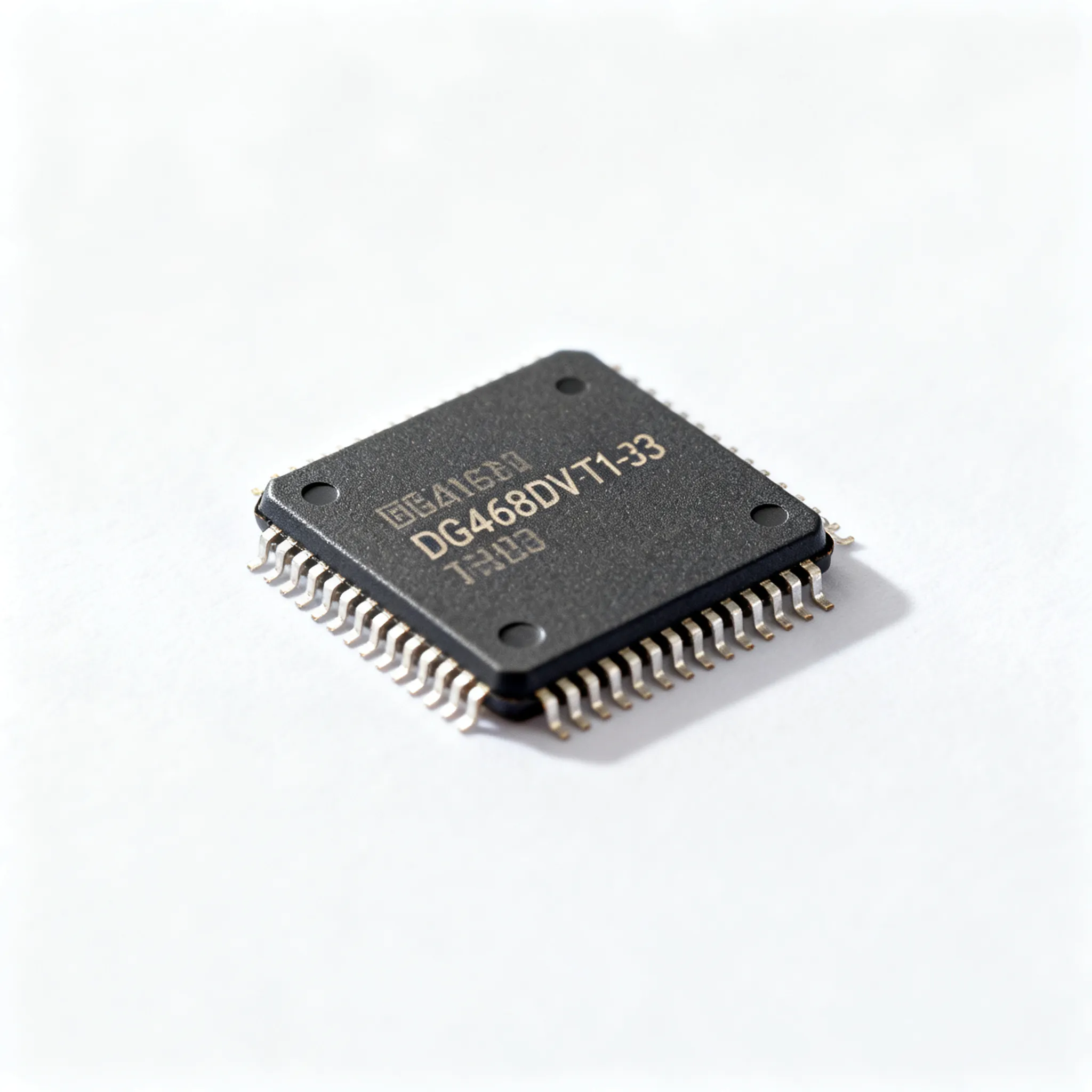
Design engineers working on battery-powered instrumentation, portable data loggers, and industrial I/O modules continue to specify DG468DV-T1-E3 because it delivers a combination of ultra‑low power and wide supply range that few single‑pole/single‑throw (SPST) switches match. With a maximum quiescent current of just 1 µA and dual‑supply operation up to ±15 V, the DG468DV-T1-E3 directly addresses the need for high‑voltage signal switching without draining the battery budget.
Distributor inventory for this Vishay part remains consistent, particularly through DigiKey, while aggregated datasheet views on alldatasheet give engineers a quick parametrics reference before diving into the full manufacturer document. This article grounds the DG468DV-T1-E3 in its datasheet essentials—pinout, key electrical performance, design trade‑offs, and sourcing checks—so you can move from evaluation to procurement with confidence.
DG468DV-T1-E3 Pinout, Internal Switch Structure, and Performance Specs
The DG468DV-T1-E3 comes in a space‑saving 6‑lead TSOP package (often referenced as SC‑59 or SOT‑23‑6). The recommended PCB footprint, according to Vishay’s CAD data, is a standard SOT‑23‑6 pattern with a 1.8 mm × 1.4 mm body size, making it easy to drop into dense layouts. Internally, the switch uses a single N‑channel MOSFET arrangement with break‑before‑make action, driven by a logic‑level input that is compatible with both TTL and 3.3 V CMOS.
Pinout Table
| Pin Number | Symbol | Function | Notes |
|---|---|---|---|
| 1 | D | Drain | Analog signal terminal; switches to Source when ON. |
| 2 | S | Source | Analog signal terminal; continuous current limited by Ron heating. |
| 3 | V‑ | Negative supply | Connect to most negative supply (0 V or negative rail). |
| 4 | IN | Logic control input | TTL/CMOS compatible; high level turns switch ON. |
| 5 | V+ | Positive supply | Maximum +15 V (referenced to V‑). |
| 6 | NC | No internal connection | Leave floating or connect to PCB ground plane. |
The truth table is straightforward: a logic high on IN closes the switch between D and S; a logic low opens it. An internal ESD protection network clamps voltage transients, but you still must respect the absolute maximum ratings—exceeding the ±18 V supply limit or injecting current beyond 30 mA can permanently damage the device. For the full cross‑section diagram and substrate details, the 13‑page, 260‑kbyte Vishay datasheet remains the authoritative source.
Key Electrical Specifications (TA = 25 °C, V+ = +15 V, V‑ = –15 V, unless noted)
| Parameter | Typical Value | Unit/Conditions |
|---|---|---|
| Switch configuration | SPST‑NO | Single channel, normally open |
| On‑resistance (Ron) | 7 | Ω at ±15 V; 9 Ω max over full temp. |
| Ron flatness | 0.5 | Ω typical over signal range |
| Supply voltage range | ±4.5 to ±15 | V (dual supply); V+ relative to V‑ |
| Quiescent supply current | 0.01 | µA typ; 1 µA max |
| Turn‑on time (ton) | 80 | ns |
| Turn‑off time (toff) | 50 | ns |
| Charge injection | 5 | pC at ±15 V |
| Off isolation | –60 | dB at 1 MHz, 50 Ω load |
| Crosstalk | Not applicable (single switch) | — |
| –3 dB bandwidth | 200 | MHz |
| Operating temperature | –40 to +85 | °C ambient |
These numbers come directly from the datasheet and from parametric summaries on Octopart. Notice the sub‑microamp supply current and the moderate on‑resistance: the DG468DV-T1-E3 prioritises power economy over ultra‑low Ron. For many precision and battery‑powered tasks, that trade‑off is exactly what you want.
Comparing the DG468 to Other SPST Switches: ADG701, TS5A3159, and On‑Resistance Trade‑offs
Engineers considering the DG468DV-T1-E3 often weigh it against other 6‑pin SPST switches that promise lower on‑resistance or tighter logic‑supply headroom. The two most relevant comparisons are the Analog Devices ADG701 and the Texas Instruments TS5A3159. While all three are housed in small‑outline SOT‑23‑6 or equivalent packages, their internal architectures and sweet spots differ significantly. Using aggregated price‑trend and inventory data from Octopart alongside official datasheets helps place each part in its proper niche.
SPST Switch Comparison
| Comparison Metric | DG468DV-T1-E3 (Vishay) | ADG701 (Analog Devices) | TS5A3159 (Texas Instruments) | Selection Criteria & Failure Boundary |
|---|---|---|---|---|
| Supply voltage range | ±4.5 V to ±15 V | +1.8 V to +5.5 V | +1.65 V to +5.5 V | If your signal exceeds 5.5 V peak, the DG468 is the only option. |
| Ron typical | 7 Ω | 2.5 Ω | 0.9 Ω | For < 100 Ω load switching, lower Ron preserves signal amplitude. |
| Ron max over temp | 9 Ω | 4 Ω | 1.5 Ω | If you must maintain < 1% gain error in a voltage divider, verify against worst‑case Ron. |
| Supply current max | 1 µA | 0.01 µA (typ), max 1 µA | 0.1 µA (typ), max 1 µA | All are micro‑power; DG468 still achieves 1 µA max at ±15 V, a notable feat. |
| Charge injection | 5 pC | 5 pC | 7 pC | In precision sample‑hold circuits, lower injection reduces pedestal error. |
| ton / toff | 80 ns / 50 ns | 12 ns / 6 ns | 25 ns / 15 ns | High‑speed multiplexing favors faster switching; DG468 targets 100 kHz–1 MHz rates. |
| Package | 6‑TSOP (SOT‑23‑6) | 6‑SOT‑23 | 6‑SC70 / SOT‑23 | Verify footprint compatibility if swapping; pinouts differ. |
| Logic threshold | TTL/CMOS at dual supply | CMOS, 1.8 V logic support | CMOS, 1.8 V logic support | DG468 logic threshold is referenced to V‑; ensure 3.3 V logic can drive high enough. |
The table makes the design boundaries clear: choose the DG468DV-T1-E3 when you must switch bipolar or high‑voltage signals up to ±12 V and cannot tolerate the extra supply current of a charge‑pump‑based level translator. The ADG701 and TS5A3159 shine in single‑supply, low‑voltage data paths where every milliohm counts, but they cannot handle signals beyond the 5.5 V rail. For the DG468, the 1 µA max quiescent current at ±15 V translates to a power draw of just 30 µW— a near‑ideal number for wireless sensor nodes and field instruments that sleep most of their life.
Design Tips, Decoupling, and Sourcing the DG468DV-T1-E3 Without Surprises
Getting the most from the DG468DV-T1-E3 demands attention to a few low‑effort PCB practices. First, always place a 0.1 µF ceramic capacitor directly across the V+ and V‑ pins, as close as physically possible to the package. The device’s internal break‑before‑make action can generate tiny supply transients during switching; that capacitor keeps local rails clean and prevents parasitic oscillation.
Sourcing guidance checklist:
- Verify suffix meaning: The ‘T1’ denotes 3,000‑unit tape‑and‑reel orientation per Vishay’s standard, while ‘E3’ confirms lead‑free (Pb‑free) RoHS compliance. Always check the reel quantity needed before issuing a PO.
- Watch the PCN: Vishay has issued a Product Change Notification concerning TSOP/SOT‑23 package orientation. Before locking in a PCB footprint, download the latest mechanical drawing from the manufacturer’s site and compare it to your CAD symbol.
- Confirm tape orientation: The T1 suffix defines a specific orientation in the carrier tape; cross‑check your pick‑and‑place programs against the datasheet outline to avoid rotated placements.
- Evaluate dual‑source alternatives as evaluation candidates, not guaranteed drop‑ins: If you evaluate pin‑compatible switches from other vendors, verify logic threshold, charge injection, and lead‑free finish. Rely on side‑by‑side testing rather than pin‑for‑pin claims.
From a procurement perspective, the DG468DV-T1-E3 is typically stocked in cut‑tape and reel quantities at DigiKey and Mouser. Use these distributors to pull live pricing and reel availability for prototypes. For production‑volume orders, submit an RFQ through IC-Online to confirm allocation‑backed lead times and flexible minimum‑order quantities. Treat the part as allocation‑sensitive during periods of high industrial demand; a buffer of 2–3 weeks’ worth of inventory has historically smoothed planning for many procurement teams.
DG468DV-T1-E3 FAQ: Real‑World Questions from Engineers and Buyers
Q: What distinguishes the DG468DV from the DG468DV-T1-E3?
The base silicon is identical. The ‘T1’ suffix indicates a 3,000‑unit tape‑and‑reel orientation per Vishay’s standard format, while ‘E3’ denotes lead‑free (Pb‑free) RoHS compliance. The bare part number, DG468DV, may refer to tube or tray packaging; always confirm the full ordering code to avoid receiving the wrong reel format.
Q: Can the DG468DV-T1-E3 switch a 12 V signal with a 3.3 V logic supply?
Yes, provided the analog supply rails accommodate the full 12 V signal swing. The logic input threshold is TTL and 3.3 V CMOS compatible, but the switch requires V+ – V‑ ≥ 13 V to pass a 12 V signal without clipping. A typical configuration uses V+ = +15 V, V‑ = 0 V, or a dual ±9 V supply. Always verify that the logic‑high level exceeds the minimum VIH at your chosen supply.
Q: Is the DG468DV-T1-E3 suitable for automotive applications?
The part is rated for an ambient temperature range of –40 °C to +85 °C and is not AEC‑Q100 qualified. It can be used in non‑safety‑critical industrial and vehicle sub‑systems, such as cabin comfort or infotainment. For under‑hood, safety‑related, or mission‑critical paths, evaluate an AEC‑qualified analog switch alternative.
Q: What are typical lead times for tape‑and‑reel orders?
When inventory is held at distributors like DigiKey or Mouser, immediate shipment is possible. For factory‑direct reel orders (3,000 pieces), lead times have historically ranged 8–10 weeks under normal market conditions, though fab allocations and demand surges can extend this. Always check real‑time lead‑time estimates on distributor portals and confirm allocation‑backed dates through an RFQ on IC-Online.
Q: How does the 5 pC charge injection affect precision analog signals?
Charge injection during switching causes a small voltage glitch at the output, typically less than 10 mV when driving a high‑impedance load. In precision data‑acquisition systems, place a unity‑gain buffer or a simple RC low‑pass filter after the switch to absorb the transient and preserve measurement accuracy. For the lowest possible glitch energy, operate at the lower end of the supply range where injection scales down.
References & Further Reading
- DG468DV-T1-E3 Full Datasheet – Vishay Siliconix (alldatasheet.com)
- DG468DV-T1-E3 at Mouser, including PCN and packaging drawings
- DigiKey product page – pricing and availability
- Octopart component comparison and distributor stock aggregation
- PCB footprint and 3D model – Vishay (via Component Search Engine)
- ADG701 Datasheet – Analog Devices
- TS5A3159 Product Folder – Texas Instruments
- Analog Switches Category – IC-Online
The DG468DV-T1-E3 earns its place on BOMs that demand high‑voltage signal routing with minimal power overhead. By understanding its precise pinout, real‑world performance specs, and the design boundaries that separate it from low‑voltage alternatives, you can confidently integrate it into your next hardware build. When you’re ready to move from evaluation to procurement, request a quote through IC-Online or upload a bill of materials for mixed‑line‑item coverage and flexible minimum order quantities. Our team will help you lock in allocation‑backed lead times without guesswork.