

How to Minimize Component Lead Times on Your BOM: Proven Strategies for Component Engineers
Practical guide for buyers and engineers: How to Minimize Component Lead Times on Your BOM: Proven Strategies for Component Engineers. Sourcing, risk, and selection notes.
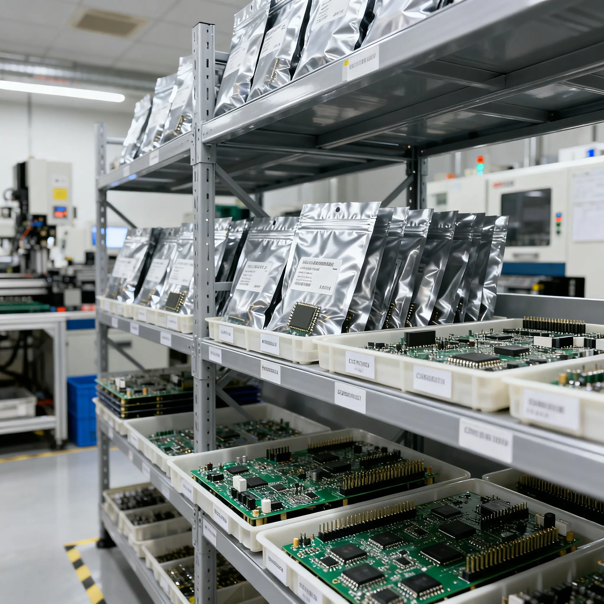
How to Slash Component Lead Times on Your BOM: A Component Engineer’s Playbook for 2026
Why 2026’s Lead-Time Crisis Is Forcing a BOM Rethink
Component engineers and procurement buyers entered 2026 knowing that the margin for error in the bill of materials had shrunk to almost nothing. The semiconductor supply chain, still digesting the aftershocks of the 2025 capacity crunch, is now dealing with a new set of constraints: AESTECHNO documents how the latest shortages are concentrated in mature-node microcontrollers, power management ICs, and high-capacitance MLCCs—categories that underpin everything from IoT gateways to EV traction inverters. The conclusion is blunt: the old habit of approving a BOM and tossing it over the wall to procurement no longer works.
What makes 2026 different is the convergence of three forces. First, single‑source ICs that once carried a predictable allocation window now routinely stretch beyond the 30‑week mark. IC Online’s 2026 shortage update puts it plainly: when a single‑source part hits that threshold, a pin‑compatible redesign is often cheaper than the cumulative risk of unverified stock. Second, the passive component market—especially MLCCs—is operating under factory load factors that force buyers to treat even “commodity” parts as allocation‑sensitive. Third, the planning horizon required to secure allocation has moved from quarters to years. GlobX advises that constrained parts now demand 18–24‑month visibility, and that categories such as MCUs, memory, and power ICs must be monitored as a group because they fail together during a shortage.
Early BOM submission is no longer a nice‑to‑have; it is the first line of defense. NextPCB highlights that a complete, accurate BOM shared with a manufacturing partner before the design is frozen allows long‑lead items to be flagged while there is still time to act—before a part becomes a build blocker. The playbook for 2026, therefore, starts with a fundamental reset: treat every BOM as a living document, and treat every component as a potential bottleneck until you have confirmed allocation‑backed lead time through a formal RFQ.
How Lead Times Harden: A BOM-Level Analysis of Component Risk
Lead time extension is rarely a gradual, predictable curve. It hardens suddenly when a wafer start is delayed, a substrate batch fails, or a factory re-allocation pushes a non‑priority device to the back of the queue. Understanding the mechanics at the BOM level helps engineers and buyers identify which lines are most likely to stall the line.
The three primary drivers of hardened lead times are demand surges from a handful of high‑volume applications, single‑source dependency that removes any negotiation leverage, and lifecycle status—specifically NRND or EOL classifications that throttle production slots. Cadence notes that real‑time lead‑time data embedded in the BOM management toolchain is essential for spotting these signals, while Odicmg argues that a lifecycle audit is the single most effective filter for pre‑empting long‑lead surprises.
Table 1 translates the 2026 landscape into a practical risk map. The lead‑time ranges shown are indicative of allocation‑backed windows reported by GlobX and other supply‑chain analysers; every figure must be confirmed via RFQ with the authorised distributor for the specific MPN and date‑code requirement.
| Component Family | Typical Allocation‑Backed Lead Time (2026) | Critical Risk Factors | Recommended Verification |
|---|---|---|---|
| 32‑bit ARM Cortex‑M MCUs (ST, NXP, Microchip, GD32‑class) | 30–52 weeks | Mature‑node wafer capacity, single‑source firmware lock‑in | Confirm allocation through franchised distributor; evaluate GD32/APM32 candidates with pin‑out and firmware verification |
| Memory ICs (DDR4, NAND flash, SPI NOR) | 20–30 weeks | OSAT capacity, cyclical demand spikes | Require allocation‑backed lead time; monitor PCN for density migrations |
| Power management ICs (DC‑DC converters, LDOs, GaN drivers) | 18–26 weeks | Fab‑node concentration, automotive‑grade priority | Verify second‑source qualification; ask distributor for factory loading status |
| High‑capacitance MLCCs (X7R/X7S, 1206–2220, ≥10 μF) | 16–24 weeks | Ceramic powder supply, regional factory allocation | Submit complete BOM early to flag long‑lead MLCCs; size‑down evaluation if possible |
| FPGAs (mid‑range, 28 nm node) | 30–50 weeks | Single‑source architecture, advanced substrate constraints | Engage supplier for provisional allocation; consider soft‑core migration path for non‑critical functions |
The table reveals a pattern: parts that share a fabrication node or a packaging substrate tend to cluster in the same risk band. A BOM that contains a 32‑bit MCU, a DDR memory, and a high‑current power stage is therefore not three independent risks—it is a single correlated risk that can halt the entire build. Adage Components reinforces that professional stocking programmes and early BOM optimisation can flatten this correlation, but only if the BOM is analysed before the procurement clock starts ticking.
Dual‑Sourcing, Buffer Stock, or Redesign: Which Tactic Fits Your BOM?
Three strategies dominate the conversation in 2026, and each solves a different version of the lead‑time problem. The art is knowing which lever to pull for which line item, because misapplying a tactic can waste engineering hours or inflate carrying costs without shrinking the risk.
Dual‑sourcing—qualifying a second source that matches form, fit, and function (FFF)—is the first line of defence for high‑runner parts. Platforms like Findchips and Supplyframe now allow engineers to filter alternates by FFF criteria during the design phase, drastically shortening the search time. However, dual‑sourcing only works when the alternate’s electrical parameters are verified against the design’s corner cases, and a pilot lot is run to confirm yield and firmware compatibility.
Strategic buffer stock bridges the gap between the moment a lead time stretches and the moment a redesign or second source is ready. In 2026, verified independent distributors that provide full traceability and test documentation have become a legitimate buffer layer—provided incoming inspection is rigorous. The risk is that buffer stock ties up working capital and can mask a single‑source problem that should have been engineered out.
Pin‑compatible redesign is the nuclear option, but one that is increasingly economical. As IC Online and Odicmg both note, when a single‑source IC exceeds 30 weeks, the cost of a small pilot redesign—including PCB re‑spin and firmware porting—is often lower than the cumulative cost of production stoppages or trusted‑broker markups. Early lifecycle analysis, as advocated by Odicmg, identifies the parts that are heading toward NRND and gives the design team time to evaluate pin‑compatible families such as GD32, APM32, or CH32‑class devices, always with the caveat that package, pin‑out, and firmware must be verified on a pilot lot.
Manufacturing scheduling also plays a supporting role. RMDB scheduling software demonstrates that reducing queue time on the shop floor can cut overall manufacturing lead times by 30–50 %, which complements the component‑side strategies by ensuring that parts that arrive late are not further delayed by production bottlenecks.
| Strategy | Component Lead‑Time Impact | Implementation Complexity | Key Risk | Best Application |
|---|---|---|---|---|
| Dual‑sourcing (FFF alternate) | Creates immediate second supply path; reduces single‑source exposure | Medium – requires electrical validation, pilot lot, and procurement onboarding | Alternate may not meet all corner‑case specs; firmware deviation possible | High‑runner MCUs, power ICs, and memory where FFF alternates are documented |
| Strategic buffer stock (via verified independent distributors) | Buys time while lead times normalise; cushions against allocation gaps | Low to Medium – depends on test protocol and traceability requirements | Working‑capital cost; risk of obsolescence if redesign is postponed | Parts with confirmed 30+ week lead times and no immediate FFF alternate |
| Pin‑compatible redesign | Eliminates dependency on the original MPN; restores negotiating power | High – involves PCB re‑spin, firmware porting, and requalification | Design cycle time; hidden firmware incompatibility | Single‑source ICs with lead times beyond 30 weeks and NRND/EOL flags |
| Manufacturing queue‑time reduction (RMDB/APS) | Does not shorten component lead time but reduces total order‑to‑ship cycle | Medium – requires integration with ERP/MES | Limited impact if component lead time is the dominant constraint | High‑mix, low‑volume production where WIP congestion adds weeks |
The decision matrix is not static. A component that starts as a buffer‑stock candidate in one quarter may become a redesign candidate the next if the supplier’s allocation window shifts. The common thread is that the decision must be made before the BOM is frozen, which is why the next section focuses on the audit‑to‑action workflow.
From Audit to Action: A Component Engineer’s Checklist for Lead‑Time Resilience
Turning the above analysis into a repeatable process is what separates organisations that ship on time from those that fight fires. The checklist below is built on practices observed in 2025‑2026 supply‑chain engagements and draws on guidance from Adage Components, Altium, and IC Online.
- Perform a lifecycle health check on every BOM line. Cross‑reference manufacturer PCN databases and distributor lifecycle alerts. Flag any part that is NRND or within 12 months of a projected EOL. If a public EOL notice exists, cite it; otherwise, verify lifecycle status via RFQ.
- Implement automated PCN/PDN monitoring. Tools such as SiliconExpert, Z2Data, and Octopart can watch the BOM and push alerts when a manufacturer changes a process, plant, or material. This is not optional for categories that fail together—MCUs, power ICs, memory, and high‑capacitance MLCCs.
- Extend the planning horizon. For any part that is single‑sourced or shows a historical lead‑time volatility, request an 18‑24‑month demand forecast from the authorised distributor and agree on an allocation buffer. GlobX warns that category‑level monitoring alone is insufficient; individual MPN forecasts are necessary.
- Submit a complete, accurate BOM to the manufacturing partner during the design phase, not after sign‑off. This allows the partner to flag long‑lead items while there is still flexibility to swap or redesign. NextPCB’s recommendation holds: early BOM submission prevents the “discovery gap” that turns a 16‑week MLCC lead time into a line‑down event.
- Consolidate part numbers where it reduces risk, not just cost. Reducing the number of unique PNs can lower the attack surface, but only if you avoid deepening dependency on a single supplier. The Altium BOM management guide suggests analysing cost‑lead‑time‑supplier triples to identify consolidation opportunities that preserve a second‑source path for the top 20 % of spend.
- Qualify independent distributor stock as bridge inventory. Work only with ISO‑certified distributors that provide full lot traceability and test reports. Require a recent (within 90‑day) test report and a maximum date code window in the RFQ. Perform incoming inspection on a sample; for high‑value or safety‑critical parts, use third‑party testing.
Table 3 distils these actions into a timeline that maps against the typical design‑to‑production cycle.
| Action | When to Use | Trade‑off |
|---|---|---|
| BOM lifecycle audit | At schematic entry and again before design freeze | Requires engineering time; may uncover redesign needs that delay the schedule, but avoids far larger delays later |
| PCN/PDN alert setup | As soon as the BOM is stable enough to export | Low effort; risk of alert fatigue if not filtered by component criticality |
| 18‑24‑month forecast sharing with distributors | For any single‑source or allocation‑sensitive part | Demand signal may be speculative; requires close buyer‑supplier trust |
| Early BOM submission to CM | During prototype build, before final BOM release | CM may flag false positives; filters need to be calibrated |
| Second‑source qualification (FFF) | For high‑runner parts where an alternate exists | Pilot lot cost and validation time; risk of firmware deviation |
The checklist is not a one‑time exercise. The 2026 procurement reality, as IC Online frames it, is that procurement is no longer about buying; it is about orchestrating a continuous flow of information between engineering, supply chain, and manufacturing. The BOM is the single source of truth for that orchestration, and the actions above keep it accurate.
Lead‑Time Questions Engineers and Buyers Ask in 2026
Q: At what lead time does a pin‑compatible redesign become cheaper than waiting for a single‑source IC?
When lead times exceed 30 weeks, as documented in the 2026 IC Online shortage update, a redesign is often cheaper than the accumulated risk of unverified stock. The cost of requalifying a new device—including a small pilot PCB run, firmware porting, and extended validation—is typically lower than the financial impact of a line‑down event or the markups charged by trusted brokers for scarce allocation. The exact threshold depends on your production volume and the cost of a stoppage, but 30 weeks is the empirical inflection point observed across multiple mid‑volume OEMs this year.
Q: How can we quickly find FFF alternates during the design phase without compromising reliability?
Use platforms like Findchips and Supplyframe that filter by form, fit, and function. These tools cross‑reference parametric data against available inventory, but they do not guarantee that the alternate will operate correctly in your specific circuit. Always verify key electrical parameters—supply voltage range, output drive, timing margins, and ESD tolerance—against your corner cases. Schedule a pilot‑lot build with the alternate before committing the second source to the production BOM, and budget for the possibility of minor firmware adjustments.
Q: What is the most effective way to validate parts from independent distributors when bridging stock?
Work only with verified, ISO‑certified distributors that provide full lot traceability and test documentation. In the RFQ, require a test report generated within the last 90 days and a maximum date code that aligns with your product’s shelf‑life policy. Upon receipt, perform incoming inspection on a statistically significant sample—visual, X‑ray if the package is suspicious, and electrical test on key parameters. For high‑value or safety‑critical parts, commission a third‑party test house to verify authenticity and performance before the parts are placed on the shelf.
Q: How do we align procurement and engineering to avoid last‑minute lead‑time surprises?
Share a complete, accurate BOM with procurement during the design phase, not after sign‑off. Hold a joint engineering‑procurement review before the BOM is frozen. During the review, flag every part that has a single‑source dependency or a known long‑lead history, agree on buffer‑stock levels, and assign ownership for second‑source evaluation. The goal is to make lead‑time risk visible to both teams before the design is locked, so that engineering can still swap a part without a costly change order.
Q: Which component categories tend to fail together during a shortage, and how should we monitor them?
MCUs, power ICs, memory, and high‑capacitance MLCCs routinely experience correlated shortages because they share fabrication and packaging supply chains. To monitor them, set automated PCN/PDN alerts on these categories using tools like SiliconExpert or Z2Data. Configure the alerts to flag any process change, node transfer, or factory re‑allocation. Pair this with an 18‑24‑month demand visibility plan shared with your authorised distributors so that allocation can be secured before the shortage becomes acute.
Q: Is it worth consolidating BOMs to fewer supplier lines to reduce lead‑time risk?
Yes, but carefully. Consolidation can reduce the number of part numbers you need to track and lower your administrative burden, but it also increases your dependency on a single supplier. If that supplier experiences a fab event or an allocation cut, the impact is magnified. Balance consolidation with dual‑source qualification for the most critical high‑value items. A practical approach is to consolidate passives and low‑criticality discretes while keeping at least two qualified sources for the top 20 % of the BOM by spend and supply risk.
References & Further Reading
Related Articles
 Blog
BlogBOM Line Risk Review: How to Vet Your Bill of Materials Before Production Release
BOM and RFQ best practices for electronic component procurement. Upload your BOM or request a quote for mixed lines and flexible MOQ.
 Blog
BlogExcess Inventory: How Component Engineers Can Turn Surplus into Supply Chain Resilience
Practical guide for buyers and engineers: Excess Inventory: How Component Engineers Can Turn Surplus into Supply Chain Resilience. Sourcing, risk, and selection notes.
 Blog
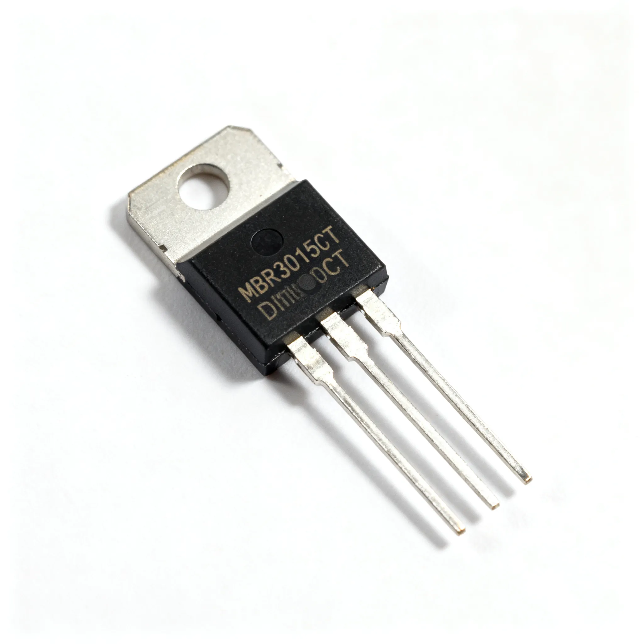
BlogMBR30150CT Supply Risk Assessment: What to Ask Before You Buy
Assess MBR30150CT sourcing risks before you buy. RFQ questions on traceability, date codes, testing, alternatives, and supply continuity for procurement teams.
 Blog
BlogUnderstanding CR2025 Equivalent Batteries and Their Industry Uses
A CR2025 equivalent includes DL2025, ECR2025, and L2025. These 3V lithium coin cells are interchangeable, matching in voltage, chemistry, and size.
 Blog
BlogUnderstanding How Graphics Cards Work in Ordinary Electronics
A definition graphics card explains how this hardware turns data into images for your screen. It's crucial for video calls, streaming, and light gaming on daily devices.
 Blog
BlogSell Excess Electronic Components: Turn OEM Inventory into Revenue
Practical guide for buyers and engineers: Sell Excess Electronic Components: Turn OEM Inventory into Revenue. Sourcing, risk, and selection notes.