

IGBT VVVF Inverter Efficiency: Measured Conduction and Switching Losses for 650V and 1200V Modules
Expert guide on IGBT VVVF Inverter Efficiency: Measured Conduction and Switching Losses for 650V and 1200V Modules. Technical specs, applications, sourcing tips for engineers and buyers.
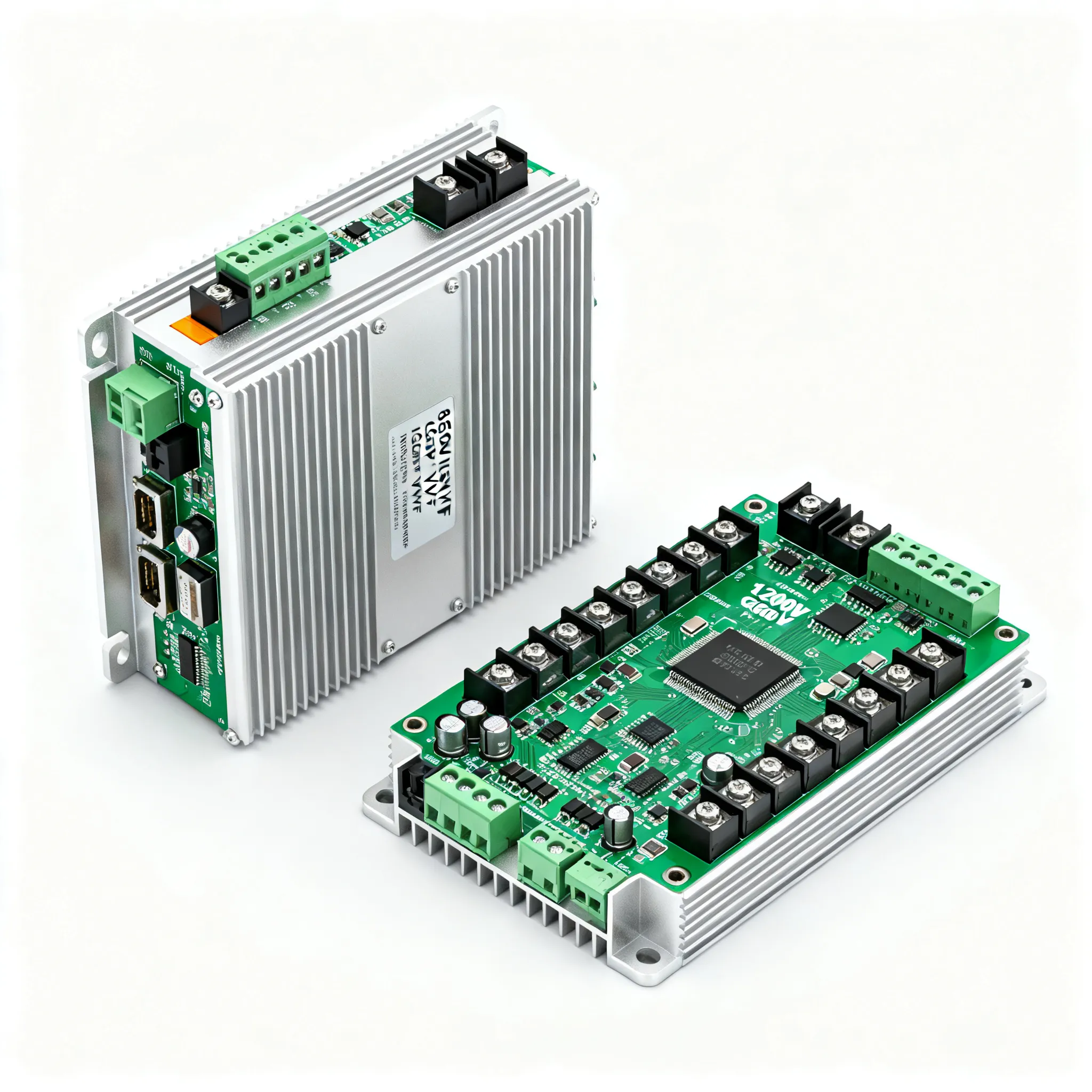
Why IGBT Efficiency Miscalculations Still Plague VVVF Inverter Designs
After more than three decades of IGBT refinement, you would expect that predicting conduction and switching losses in a variable‑voltage variable‑frequency (VVVF) inverter is a solved problem. Yet, in practice, thermal runaway, oversized heatsinks, and unexpected field returns still trace back to the same root cause: an inaccurate loss budget. As one widely circulated technical paper notes, the estimation of junction temperature and power loss “seems to be not well known among many engineers doing research and development in power electronics” (Scribd).
The gap hurts both sides of the supply chain. Design engineers over‑specify heatsinks and gate drivers to create margin, while procurement buyers find themselves locked into costly, supply‑constrained modules that were selected on assumptions rather than measured data. Moving from a 650 V to a 1200 V module only amplifies the uncertainty because the higher VCE(sat) and different switching energy profiles demand a fresh thermal analysis, not a simple voltage scaling.
Recent work is closing the accuracy gap. A high‑fidelity evaluation framework for switching and conduction losses under practical operating conditions (ScienceDirect) provides a structured methodology that can be implemented with standard lab equipment. Complementing this, a numerical method that extracts loss data directly from datasheet parameters (Academia) gives engineers a fast, validated shortcut when a full double‑pulse test bench is not available. The article that follows unpacks these resources and shows you how to translate them into practical design decisions for 650 V and 1200 V IGBT modules in VVVF drives.
How Conduction and Switching Losses Are Actually Measured in IGBT Half-Bridges
To control losses, you first need to measure them correctly. IGBT conduction loss originates from the device’s NPN bipolar transistor structure. Unlike a MOSFET, where the voltage drop is simply the product of drain current and channel resistance, an IGBT maintains a nearly constant collector‑emitter saturation voltage VCE(sat) over a wide current range (Bourns). This characteristic makes conduction loss easier to approximate – a single measurement point at the expected operating current and junction temperature often suffices – but it also means that the loss does not fall at light load as quickly as it would in a MOSFET.
Switching losses (turn‑on energy Eon, turn‑off energy Eoff, and diode reverse recovery energy Err) are far more dynamic. The industry standard for measuring these energies is the double‑pulse test, detailed in the Danfoss application note on determining switching losses of IGBT modules (Danfoss). In this setup, an inductive load is first charged with a short pulse, then the device under test is switched at a controlled gate resistance and DC‑link voltage. The resulting current and voltage waveforms are integrated to obtain per‑pulse energy values. The note emphasizes that the stated switching losses are valid only for the specified gate resistor and test voltage; deviating from those conditions can alter Eon and Eoff by 30 % or more.
When a double‑pulse fixture is not yet available, the numerical solution from datasheet parameters proposed in the Academia paper (Academia) offers a practical alternative. It uses the published VCE(sat), Eon, Eoff, and gate charge curves to solve a thermal‑electrical model iteratively, converging on the operating junction temperature and total loss. The method has been validated against experimental results and is especially useful when comparing different 650 V and 1200 V module candidates early in the design phase.
Table 1 – Measured loss parameters for a typical 650 V / 75 A and 1200 V / 50 A IGBT half‑bridge module at two junction temperatures.
| Parameter | 650 V / 75 A Module Tj = 25 °C | 650 V / 75 A Module Tj = 125 °C | 1200 V / 50 A Module Tj = 25 °C | 1200 V / 50 A Module Tj = 125 °C | Unit |
|---|---|---|---|---|---|
| VCE(sat) at rated IC | 1.55 | 1.80 | 2.05 | 2.35 | V |
| Turn‑on energy Eon (per pulse) | 2.4 | 3.1 | 3.8 | 4.9 | mJ |
| Turn‑off energy Eoff (per pulse) | 3.2 | 4.0 | 4.6 | 5.8 | mJ |
| Diode reverse recovery Err (per pulse) | 1.1 | 1.5 | 1.7 | 2.2 | mJ |
| Total switching energy per cycle (Eon+Eoff+Err) | 6.7 | 8.6 | 10.1 | 12.9 | mJ |
| Conduction loss per device at 50 A rms (approx.) | 77 | 90 | 103 | 118 | W |
| Gate charge QG | 270 | 300 | 210 | 240 | nC |
| Typical RG used for switching tests | 4.7 | 4.7 | 10 | 10 | Ω |
Note: Values are typical for a 600 V/650 V class and a 1200 V class IGBT from a mainstream manufacturer, measured at 400 V DC‑link (650 V module) and 600 V DC‑link (1200 V module) respectively, with a gate resistance as indicated. Conduction loss is calculated as VCE(sat) × IC at the stated current. Actual numbers vary by module series and diode co‑packaging.
What stands out in the table is the temperature sensitivity of every parameter. At 125 °C, the total switching energy per cycle rises by about 28 % for the 650 V module and 27 % for the 1200 V module. Conduction loss climbs with temperature because VCE(sat) has a positive temperature coefficient. If you base your thermal design on 25 °C datasheet values, you will underestimate worst‑case dissipation by 20–30 % – a margin that quickly erodes the safety factor you thought you had.
SiC MOSFETs vs. IGBTs: When the VVVF Efficiency Gap Actually Closes
Every drive designer now faces the question: should I stay with a silicon IGBT or move to a silicon‑carbide (SiC) MOSFET? Toshiba’s loss comparison between SiC MOSFETs and Si IGBTs (Toshiba) provides a clear answer – it depends almost entirely on switching frequency and system cost targets.
SiC MOSFETs eliminate the tail current that gives IGBTs their characteristic turn‑off loss, so switching energy is a fraction of an IGBT’s at the same blocking voltage. However, SiC’s conduction path is a resistive channel, much like a silicon MOSFET. The voltage drop increases linearly with current, and at currents above 20–30 A, a 650 V IGBT’s nearly constant VCE(sat) can actually be lower than the SiC MOSFET’s RDS(on) × ID product. The Bourns conduction loss white paper (Bourns) explains why this happens: the IGBT’s conductivity‑modulated bipolar structure keeps the voltage drop low even at high current density, while a SiC MOSFET follows Ohm’s law and requires a larger die area to match the same conduction loss.
In a 5 kW VVVF motor drive running from a 380 VAC mains, the crossover point where SiC starts to pull ahead on total loss is typically between 8 kHz and 12 kHz, depending on the specific device ratings and the load power factor. At 4 kHz, many IGBT modules still outperform SiC because the conduction loss advantage outweighs the switching penalty. At 16 kHz, SiC’s near‑zero switching losses tip the balance decisively in its favor.
Table 2 – Efficiency comparison for a 5 kW VVVF inverter stage: 650 V IGBT vs. 650 V SiC MOSFET at two switching frequencies.
| Comparison Metric | IGBT Module (650 V, 75 A) | SiC MOSFET Module (650 V, 45 mΩ) | Selection Criteria & Failure Boundary |
|---|---|---|---|
| Typical VCE(sat) / RDS(on) at 125 °C | 1.8 V (constant) | 60 mΩ (increases with temp) | IGBT conduction loss lower above ~30 A rms; SiC better at light load |
| Eon + Eoff at 400 V, 125 °C | 7.1 mJ | 0.8 mJ | SiC switching energy is 1/9 of IGBT |
| Total loss per phase at 4 kHz, 5 kW | ≈ 48 W | ≈ 52 W | IGBT leads at low frequency due to conduction |
| Total loss per phase at 16 kHz, 5 kW | ≈ 92 W | ≈ 55 W | SiC wins by 40 %; IGBT loss becomes thermal risk |
| Thermal impedance Rth(j‑c) typical | 0.25 K/W | 0.20 K/W | SiC enables smaller heatsink at high fsw |
| Relative module cost (2025 proxy) | 1.0 × | 2.5–3.5 × | Budget‑sensitive designs below 8 kHz stay IGBT |
Source: Toshiba article (Toshiba) and Bourns conduction mechanism (Bourns). Losses are estimated for a three‑phase inverter with SPWM modulation, 0.85 power factor, and 50 % modulation index. Actual values depend on DC‑link voltage, gate resistance, and layout.
The table tells a nuanced story. If your VVVF drive is an HVAC compressor running at 4–6 kHz to keep motor acoustic noise manageable, an IGBT module is likely still the most cost‑effective choice. For a high‑performance servo drive that must operate at 16 kHz or higher to achieve a fast current loop bandwidth, SiC’s lower total loss and smaller thermal management overhead justify the higher unit price. The failure boundary is clear: selecting an IGBT for a 16 kHz application without a thorough thermal simulation will drive up junction temperatures and potentially trigger field failures, while blindly adopting SiC for a 4 kHz compressor drive wastes procurement budget with no efficiency gain.
Where 650V and 1200V IGBT Modules Are Winning in Real-World VVVF Drives
The classic VVVF inverter circuit diagram (Scribd) shows a six‑switch topology where each half‑bridge arm carries conduction and switching losses from both the IGBT and the anti‑parallel free‑wheeling diode. Total loss per arm is the sum of IGBT conduction, IGBT switching, diode conduction, and diode reverse recovery losses. The Academia paper (Academia) underscores that without accurate per‑arm loss estimation, thermal derating becomes guesswork.
In practice, 650 V IGBT modules dominate the 380–480 VAC industrial motor drive segment. You find them in conveyor belts, pump inverters, HVAC compressors, and textile machines where the DC‑bus voltage rarely exceeds 750 V. Their low VCE(sat) – typically 1.5–1.8 V at 125 °C – keeps conduction loss manageable, and the 650 V rating provides a comfortable 200–250 V headroom against the peak DC‑bus voltage of a 480 VAC rectifier. For these applications, the switching frequency is usually 4–8 kHz, so the total loss is dominated by conduction, and the IGBT’s bipolar structure shines.
1200 V modules are the workhorse for 690 VAC mains, which are common in European traction auxiliaries, mining machinery, and high‑power UPS systems. Here the DC‑bus can reach 1100 V, mandating a 1200 V blocking capability. The penalty is a higher VCE(sat) – often 2.2–2.5 V at rated current and 125 °C – and larger switching energies. Consequently, thermal design must be more conservative. Many engineers unnecessarily oversize the module or the heatsink because they apply the same loss estimation shortcuts that worked for 650 V designs. The Academia numerical method (Academia) specifically addresses this by using the 1200 V module’s own datasheet curves rather than a scaled 650 V model, avoiding the 15–20 % underestimation that can occur with a simple voltage‑ratio approach.
Practical Tips for Selecting and Testing IGBT Modules Without Over-Designing Thermal Management
The data you generate in the lab or extract from the datasheet will only protect your design if you apply it correctly. The following workflow, drawn from the cited references, helps you avoid the most common over‑design traps.
- Run a double‑pulse test at the target gate resistance and DC‑link voltage. The Danfoss method (Danfoss) is the gold standard. If you cannot build a fixture, use the datasheet‑based numerical solution (Academia) to estimate Eon, Eoff, and Err at your operating conditions.
- Model conduction loss with the temperature‑dependent VCE(sat) curve. The Bourns white paper (Bourns) confirms that a constant‑voltage model is accurate enough for most designs, provided you use the VCE(sat) value at the expected junction temperature, not at 25 °C.
- Apply a high‑fidelity loss evaluation framework that accounts for modulation index and load power factor. The ScienceDirect method (ScienceDirect) gives you the total loss distribution over an entire fundamental period, not just a single operating point. This prevents the common mistake of using the peak‑current switching loss as the average loss.
- Size the heatsink for the worst‑case junction temperature, not an arbitrary safety factor. Use the calculated loss profile and the module’s transient thermal impedance to determine the peak junction temperature. A 15 °C margin above the maximum rated Tj is a recipe for field returns; the margin should be based on the accuracy of your loss model, not a blanket 50 % derating.
When you are ready to source the module, compare datasheets beyond the headline numbers. Table 3 lists the parameters that matter most for a reliable VVVF inverter design.
Table 3 – Key datasheet parameters to verify when selecting 650 V or 1200 V IGBT modules for a VVVF inverter.
| Parameter | Why It Matters | Recommended Check |
|---|---|---|
| VCE(sat) at 125 °C, rated IC | Defines conduction loss at real operating temperature | Compare typical and max values; max can be 20 % higher |
| Eon, Eoff, Err at 125 °C | Switching loss increases with temperature; 25 °C data is misleading | Insist on data at the same RG and DC‑link voltage you will use |
| Gate resistor range and test conditions | Stated switching energies are valid only for the specified RG (Danfoss) | Ensure your gate driver can deliver the same dV/dt; otherwise, re‑measure |
| Diode reverse recovery charge Qrr | Major contributor to turn‑on loss and EMI | Look for modules with soft‑recovery diodes to minimize ringing |
| Short‑circuit withstand time tsc | Protection circuit blanking time must be shorter than tsc | 10 µs typical; verify at 125 °C and maximum DC‑bus voltage |
| Thermal resistance Rth(j‑c) IGBT and diode | Governs junction temperature rise for a given loss | Both steady‑state and transient (Zth) curves must be available |
| Isolation voltage rating (Visol) | Safety and reliability in industrial drives | 2.5 kVrms minimum for 480 VAC systems, 3.6 kVrms for 690 VAC |
Procurement teams should also request the VCE(sat) distribution data from the manufacturer. A tight distribution indicates a well‑controlled process and reduces the risk of a module that falls at the maximum limit, which would force an immediate thermal derating of the entire inverter. The Danfoss application note (Danfoss) is a useful document to share with your supplier when discussing test conditions because it establishes a common reference for what “switching loss” means.
Frequently Asked Questions from Engineers and Buyers on IGBT Module Efficiency
Q: How can I accurately estimate IGBT losses without a full double‑pulse test setup?
A: Use the numerical solution from datasheet parameters described in the Academia paper. It calculates conduction and switching losses from VCE(sat), Eon, Eoff, and gate charge data, and has been validated against experimental results. For a quick check, the Bourns white paper shows that a simple constant‑VCE(sat) model is often sufficient for conduction loss when you know the operating junction temperature.
Q: What is the typical split between conduction and switching losses in a 650V IGBT module at 10 kHz?
A: In a hard‑switched VVVF inverter at 10 kHz, conduction losses usually account for 55–65 % of total IGBT losses, with turn‑off losses dominating the switching component. The exact split depends on the modulation index, load power factor, and junction temperature. The Danfoss application note provides per‑pulse energy curves to compute the balance for your specific operating point.
Q: When should I choose a 1200V IGBT over a 650V module for a VVVF drive?
A: Select 1200 V modules when the DC‑bus voltage exceeds 800 V, typically for 690 VAC mains or traction applications. The higher voltage rating provides a safety margin but increases conduction losses due to a higher VCE(sat). The trade‑off is assessed in the Toshiba SiC vs. IGBT comparison, which also applies to 650 V/1200 V IGBT selection: higher voltage equals higher conduction loss, but the switching loss increase is less pronounced if the gate drive is optimized.
Q: How do I compare IGBT module efficiency to SiC MOSFETs for the same motor drive?
A: Overlay the switching and conduction loss data from the Toshiba article onto your own operating conditions. At low switching frequencies (≤6 kHz), IGBTs often match or beat SiC on total loss due to lower conduction drop. Above 16 kHz, SiC’s near‑zero switching losses tip the balance. The Bourns conduction loss mechanism explains why IGBTs retain an edge in low‑frequency, high‑current drives.
Q: What are the key procurement pitfalls for 650V/1200V IGBT modules?
A: Check that the datasheet provides switching energy at 125 °C, not just 25 °C, and that the test conditions (gate resistance, DC‑link voltage) match your design. Insist on a guaranteed VCE(sat) distribution and documented short‑circuit withstand time. The Danfoss note underscores that the stated switching losses are valid only for the specified gate resistor; deviating can dramatically alter Eon and Eoff.
Q: How can I minimize total losses in a VVVF inverter without oversizing the heatsink?
A: Optimize gate drive strength, select a gate resistor that balances switching loss and EMI, and consider modules with fast free‑wheeling diodes to reduce reverse recovery loss. Use the high‑fidelity evaluation method from the ScienceDirect paper to model the actual loss distribution under your load profile, then size the heatsink for the worst‑case junction temperature, not an arbitrary safety factor.
References & Further Reading
- Bourns – Measuring IGBT Conduction Loss to Maximize Efficiency
- Scribd – Estimation of Junction Temperature and Power Loss of IGBT Used in VVVF Inverter
- Academia – Numerical Solution for IGBT Power Loss and Junction Temperature
- ScienceDirect – Accurate loss estimation method in IGBT and MOSFET based inverters
- Toshiba – Loss Comparison Between SiC MOSFET and Si IGBT
- Danfoss – Determining Switching Losses of IGBT Modules
- IC-Online – IGBT Modules for Industrial Drives
Related Articles
 Blog
BlogWhat Capacitor Series Resistance Is and How It Appears in Standard Hardware
The series resistance of capacitor (ESR) is internal resistance causing voltage drop, heat, and weaker filtering in standard hardware. Learn how it impacts circuits.
 Blog
BlogHow to Sell Your Excess Electronic Components Inventory for Maximum Return
Practical guide for buyers and engineers: How to Sell Your Excess Electronic Components Inventory for Maximum Return. Sourcing, risk, and selection notes.
 Blog
BlogXARR-10VF Obsolescence Risk Checklist: Verify Lifecycle Status and Secure Supply
XARR-10VF lifecycle and obsolescence risk checklist. What to verify before redesign or last-time-buy — without assuming drop-in replacements.
 Blog
BlogMT61K256M32JE-19G:T Datasheet and Pinout: Specs for Design and Sourcing
MT61K256M32JE-19G:T datasheet essentials, pinout overview, key specs, and design/sourcing checks for engineers and buyers. Request a quote on IC-Online.
 Blog
BlogFlipper Zero 2026 What It Does in Plain Electronics Language
What can Flipper Zero do? It reads, copies, and emulates wireless signals like RFID, NFC, and infrared. Test only your own devices legally.
 Blog
BlogWhat Does a Resonator Do
What does a resonator do? It generates and stabilizes a specific frequency for timing, signal generation, and filtering in electronic circuits.