ISO122P: What This Isolation Amplifier IC Is, How It Works, and When to Use It
If you need to move an analog signal from a “noisy” or high-voltage domain to a safe, low-voltage domain without sharing gro
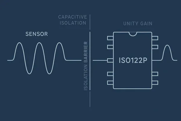
If you need to move an analog signal from a “noisy” or high-voltage domain to a safe, low-voltage domain without sharing ground, an isolation amplifier is often the simplest answer. ISO122P is Texas Instruments’ PDIP version of the ISO122, a unity‑gain, precision isolation amplifier that sends analog signals across a capacitive isolation barrier. In short, it breaks ground loops and protects downstream electronics while reproducing the input at 1 V/V on the other side, within its specified bandwidth and linearity.
According to the device overview, ISO122 provides a 1500 Vrms isolation withstand, roughly 50 kHz small‑signal bandwidth, and around 0.020% maximum nonlinearity in unity gain, all documented in the family’s collateral on the Texas Instruments ISO122 product page and the current PDF on the TI ISO122 datasheet landing page.
The quick definition (and why it exists)
- ISO122P = ISO122 in a 16‑pin plastic DIP (PDIP) package. The “P” suffix denotes the package. See TI’s orderable device details via the TI ISO122P device page.
- Functionally: a precision, unity‑gain isolation amplifier. It transfers an analog voltage across an internal capacitive barrier and reconstructs it on the output side with high linearity.
- Purpose: eliminate shared ground paths that cause ground loops, reduce risk from high common‑mode voltages, and protect low‑voltage measurement stages.
Use it when you need an analog signal on the far side of an isolation barrier and you don’t want to design your own transformer/optocoupler analog link.
How ISO122P works (high level)
Inside the chip, the input voltage is converted into a high‑frequency duty‑cycle modulated waveform. That modulated signal crosses a differential capacitive barrier (on the order of a couple of picofarads). On the secondary side, ISO122 demodulates and filters the waveform back into an analog voltage at unity gain. TI describes this duty‑cycle modulation/demodulation approach and the barrier structure in the device’s functional description on the TI ISO122 datasheet landing page.
Design implications:
- Expect a small residual switching ripple at the output. TI recommends a simple low‑pass post‑filter to reduce it while preserving bandwidth; see TI’s guidance in the application report on ISO12x output filtering, the TI app report SBOA012.
- Each side of the isolation barrier needs its own local, isolated supply rails. Proper decoupling on both sides is essential; TI’s datasheet shows recommended practices on the TI ISO122 datasheet landing page.
Key parameters (what they mean in practice)
- Isolation withstand: ISO122 is production‑tested to 1500 Vrms isolation. This is a device‑level withstand rating, not a system safety certification; TI explains isolation terminology and how to interpret ratings in its technical note “Understanding isolation terminology” (SLYT676) from 2025 and prior revisions.
- Bandwidth: about 50 kHz small‑signal bandwidth. For most industrial sensors, 50/60 Hz line signals, and many control loops, that’s sufficient. If you need wider bandwidth or very low ripple/noise, consult alternatives below.
- Linearity: on the order of 0.020% max. For mid‑precision analog links, that is usually ample; for metrology‑level precision, consider tighter‑linearity options.
- Supply rails: dual supplies on each side (roughly ±4.5 V to ±18 V), with typical input/output ranges around ±10 V. Verify exact limits versus rails in the latest Electrical Characteristics tables on the TI ISO122 datasheet landing page.
- Package: ISO122P is the PDIP option, useful for through‑hole or legacy boards; SOIC variants exist in the same family if you prefer surface‑mount, listed on the Texas Instruments ISO122 product page.
What ISO122P is not (boundary check)
- Not a digital isolator or an isolated ADC. ISO122P outputs an analog voltage; there’s no digital bitstream or SPI/I2C involved.
- Not a medical certification in a chip. The 1500 Vrms device‑level rating doesn’t equate to reinforced isolation or end‑equipment compliance by itself. System‑level safety depends on creepage/clearance, PCB layout, supply architecture, and standards testing, as TI discusses in SLYT676 on isolation terminology.
Typical applications
- Industrial measurement and control: isolated sensor interfaces for PLCs/DAQ modules to break ground loops and reject high common‑mode voltage. See device positioning on the Texas Instruments ISO122 product page.
- Power and energy systems: high‑side shunt current sensing, isolated voltage monitoring for battery stacks or motor drives.
- Laboratory and medical‑adjacent instruments: patient‑isolated analog front ends where the system, not the chip alone, achieves certification.
In short: choose ISO122P when you need a clean, unity‑gain analog hop across an isolation barrier with mid‑bandwidth, mid‑precision requirements and a convenient PDIP package.
Design‑in checklist (practical tips)
- Power both sides separately: Provide isolated supplies for input and output domains; decouple each side with a 0.1 µF ceramic close to the pins and an appropriate bulk capacitor.
- Filter the ripple: Add a modest low‑pass post‑filter on the output to knock down demodulator ripple without sacrificing your target bandwidth; TI’s SBOA012 filter note has practical guidance.
- Respect input/output ranges: Keep the signal within the linear input range and ensure the output has headroom relative to its supply rails; check the curves in the latest PDF on the TI ISO122 datasheet landing page.
- Layout the barrier like a barrier: Maintain creepage/clearance across the isolation gap on your PCB. Keep high‑dv/dt nodes away from sensitive inputs.
- Plan for drift and temperature: For precision systems, budget offset, drift, and ripple; verify numbers from the datasheet’s Electrical Characteristics table during your error budget.
ISO122P vs alternatives (when to pick what)
- ISO124 (same family, tighter linearity): If you want a pin‑compatible, unity‑gain device with lower nonlinearity (around 0.010% max in the family specs), consider the sibling noted on the TI ISO124 product page. It offers similar bandwidth with improved precision.
- ISO224 (modern isolated amplifier): For higher isolation ratings, improved noise/linearity, and modern supply options, evaluate devices like ISO224 described on the TI ISO224 product page. These are purpose‑built for newer designs.
- Delta‑sigma based isolated amplifiers (digital output): If you plan to feed a microcontroller or ADC directly with a digital bitstream and want reinforced isolation options and excellent accuracy, look at AMC13xx/AMC33xx families in TI’s isolated amplifiers portfolio overview.
Selection guidance:
- Maintain/retrofit with minimal redesign and need PDIP: ISO122P.
- Same topology, higher precision: ISO124.
- New design, tighter accuracy or higher isolation, or digital interface preferred: ISO224 or AMC13xx/AMC33xx families.
Example use cases (textual sketches)
- Isolated 4–20 mA loop receiver: Convert the loop current to voltage with a resistor on the input side, pass it through ISO122P at unity gain, and then low‑pass filter before the MCU’s ADC on the safe side.
- High‑side shunt current sensing: Sense millivolts across a shunt in a motor drive, amplify as needed before ISO122P if required, transfer across the barrier, then condition and digitize.
- Ground‑loop breaker for lab DAQ: Isolate a sensor or transducer whose ground is offset or noisy relative to the acquisition system.
FAQs
- Can ISO122P run from a single supply? The architecture is typically used with dual supplies on both sides; check the datasheet for permissible single‑supply operation modes and limitations on the TI ISO122 datasheet landing page.
- What bandwidth and accuracy should I expect? About 50 kHz small‑signal bandwidth and roughly 0.020% max nonlinearity are presented in the device overview on the Texas Instruments ISO122 product page. Verify the exact limits and test conditions in the latest PDF.
- Is it medically certified by itself? No. The chip provides galvanic isolation with a 1500 Vrms withstand rating, but system‑level standards compliance requires full end‑equipment design and testing per guidance such as TI’s SLYT676 on isolation terminology.
- How do I reduce output ripple? Add a modest low‑pass filter as suggested in TI’s SBOA012 filtering app report, tuned to your bandwidth needs.
- Is ISO122P still available? As of 2025, the device family remains documented by TI; check current status and stock on TI and distributors like Mouser and Digi‑Key. See TI’s orderable view on the TI ISO122P device page and verify listings such as Mouser’s ISO122P page or Digi‑Key’s ISO122P detail page on your purchase date.
Bottom line
ISO122P is a workhorse analog isolation amplifier: simple unity‑gain transfer, mid‑bandwidth performance, and a PDIP package for through‑hole or legacy builds. It shines when you need a straightforward, galvanically isolated analog link without moving to digital bitstreams or more complex signal paths. For higher precision or newer isolation requirements, TI’s ISO124, ISO224, or delta‑sigma‑based alternatives are ready options—but when you want a proven, PDIP unity‑gain isolator, ISO122P remains a solid choice backed by TI’s documentation on the ISO122 product page and the current datasheet landing.