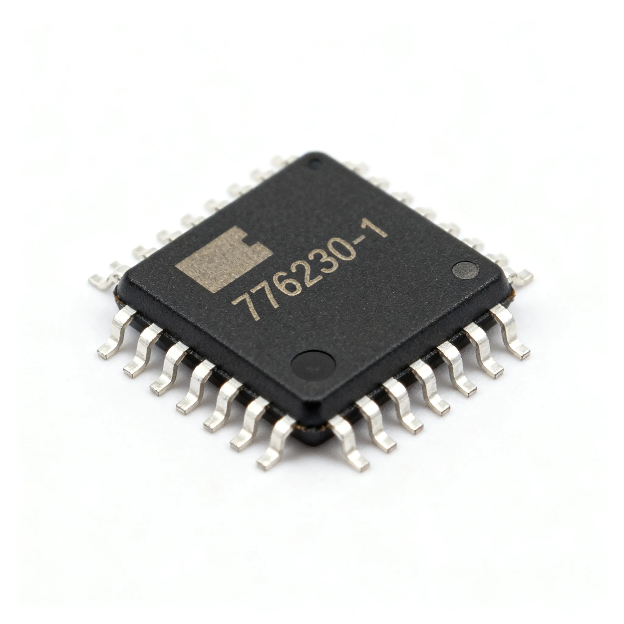
LE25U40CMDTWG Datasheet and Pinout: Specs for Design and Sourcing
LE25U40CMDTWG datasheet essentials, pinout overview, key specs, and design/sourcing checks for engineers and buyers. Request a quote on IC-Online.
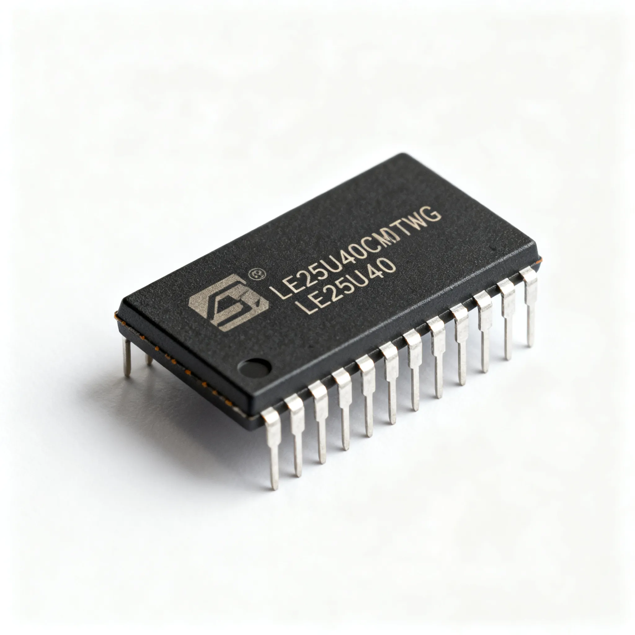
LE25U40CMDTWG Datasheet and Pinout: Specs for Design and Sourcing
Why the LE25U40CMDTWG Stays on the BOM Despite an Evolving NOR Flash Market
Serial NOR flash in the 4‑Mbit density class hasn’t disappeared, but the supplier landscape has narrowed. Several legacy parts have entered “last‑time‑buy” status or require allocation‑backed ordering, leaving design teams scrambling for a reliable, long‑life component that doesn’t force a board respin. The LE25U40CMDTWG from onsemi remains a pragmatic choice precisely because it’s still actively listed at franchised distributors such as Mouser and Newark Electronics, and is widely referenced by procurement platforms like Jotrin Electronics. That continuity gives engineers confidence to lock the part into field‑upgradable boot‑code and configuration storage designs.
The device stands out because it runs from a single 2.5 V supply — a voltage domain still common in FPGA banks, low‑power MCUs, and industrial sensor nodes. Where 3.3‑V‑only NOR flash would force an additional LDO or a dedicated rail, the LE25U40CMDTWG integrates naturally, saving board space and simplifying power sequencing. Coupled with an industrial temperature range of –40 °C to +85 °C, it covers the majority of factory‑floor and outdoor telemetry applications without derating.
Note: While the part continues to flow through authorized channels, any serial NOR flash should be treated as allocation‑sensitive in today’s market. Verify current availability and obtain an allocation‑backed lead‑time quote through your distributor or via an RFQ on IC-Online before freezing the bill of materials.
Decoding the Datasheet: LE25U40CMDTWG Pinout, Voltage, and AC Timing
A close reading of the official ON Semiconductor datasheet reveals a 4‑Mbit array organized as 512K × 8 bits, accessed through standard SPI or Dual SPI commands. The memory operates on a VCC range of 2.3–2.7 V, with an access time of 11 ns that permits serial clock frequencies up to 85 MHz in single‑bit read mode. The device supports uniform 4‑KB sectors and a deep power‑down mode that draws less than 5 µA, critical for battery‑backed data loggers that wake periodically to dump a sensor buffer.
The 8‑pin SOIC package (SOIC‑N, 150‑mil body) follows the industry‑standard pinout for SPI NOR flash:
- Pin 1 (CS#): Chip Select – active low; pulled high internally.
- Pin 2 (SO / IO1): Serial Data Output in SPI mode; bidirectional IO1 in Dual SPI mode.
- Pin 3 (WP# / IO2): Write Protect active low when not in Dual SPI; functions as IO2 in Dual SPI quad‑IO reads (note the part is Dual SPI, not Quad SPI).
- Pin 4 (GND): Ground reference.
- Pin 5 (SI / IO0): Serial Data Input in SPI mode; bidirectional IO0 in Dual SPI mode.
- Pin 6 (SCK): Serial Clock input.
- Pin 7 (HOLD# / IO3): Hold active low to pause a transaction; in Dual SPI mode this pin acts as IO3, though the datasheet generally restricts dual‑IO operations to two lines (IO0/IO1). Verify the Dual SPI command subset to avoid unexpected behaviour.
- Pin 8 (VCC): 2.3–2.7 V supply.
This pinout is footprint‑compatible with the vast majority of 8‑SOIC NOR flash memories from Winbond, Macronix, and Microchip, which simplifies second‑source risk evaluation — though pin‑function compatibility alone does not guarantee software drop‑in readiness, as command‑set and status‑register layouts differ.
Engineers should pay attention to the HOLD#/WP# dual‑role pins. In Dual SPI mode the device effectively breaks the dedicated write‑protect and hold functions. If your system requires hardware write protection during power‑up or brown‑out events, you must either stay in single‑SPI mode or replicate that protection in an external supervisor circuit.
Key Specifications at a Glance
| Parameter | Value / Range | Unit & Notes |
|---|---|---|
| Density | 4 Mbit (512K × 8) | Uniform 4‑KB sectors |
| Supply Voltage (VCC) | 2.3 – 2.7 | V; absolute maximum 3.0 V |
| Interface | SPI (single) / Dual SPI | Supports Fast Read dual‑output (3Bh) and dual‑IO (BBh) commands in the dual‑SPI subset; no Quad SPI support |
| Maximum Clock Frequency (fSCK) | 85 MHz (single‑bit read) | 11 ns access time, dependent on dummy‑byte count |
| Deep Power‑Down Current | 5 µA (max) | Typical values lower; wake‑up time 3 µs |
| Program / Erase Cycles | 100,000 cycles per sector | Endurance rating across full temperature range |
| Data Retention | 20 years minimum | At 55 °C; longer at lower temperatures |
| Temperature Range | –40 to +85 °C | Industrial; “C” suffix denotes commercial/industrial grade |
| Package | 8‑pin SOIC‑N (150 mil) | Tape‑and‑reel suffix “TWG”; lead‑free, RoHS |
| Programming Granularity | Byte / Page (256‑byte program buffer) | Typical page‑program time 3 ms |
From the spec table you can see the device is sharply optimised for low‑voltage, moderate‑speed code shadowing. If your SPI controller can sustain a 40‑50 MHz clock with clean timing margins, the flash will deliver boot‑code reads in a fraction of a millisecond. However, the absence of quad‑IO means that high‑throughput data‑logging applications with multi‑megabit‑per‑second requirements should look to the Macronix MX25L8035E or similar quad‑capable parts — a trade‑off discussed in the next section.
When to Pivot from the LE25U40CMDTWG: Microchip and Macronix Alternatives
While the LE25U40CMDTWG fills the 2.5‑V, industrial 4‑Mbit slot well, PCB design and supply‑chain dynamics frequently demand a backup. Cross‑referenced alternatives typically come from Microchip’s SST25VF family and Macronix’s MX25L series. A side‑by‑side comparison extracted from Octopart’s parametric search and distributor listings helps quantify the engineering trade‑offs.
| Comparison Metric | LE25U40CMDTWG (onsemi) | SST25VF010A-33-4I-SAE (Microchip) | MX25L8035EM2I-10G (Macronix) | Selection Criteria & Failure Boundary |
|---|---|---|---|---|
| Density | 4 Mbit | 1 Mbit | 8 Mbit | Density must cover firmware size + overhead for OTA updates. Switching to 1 Mbit often requires code pruning. |
| Supply Voltage | 2.3 – 2.7 V | 2.7 – 3.6 V | 2.7 – 3.6 V | Any move to 3.3‑V flash demands a voltage rail that may not exist in a pure 2.5‑V system — budget for a regulator or level translator. |
| Interface | SPI / Dual SPI | SPI | SPI / Dual SPI / Quad SPI | Quad‑IO can cut read time for boot images but requires 2 extra MCU pins and careful layout of four high‑speed lines. |
| Max Single‑Bit Clock | 85 MHz | 33 MHz | 104 MHz | Above 40 MHz, PCB trace length and capacitance become dominant. A 33‑MHz limit may force a slower boot on the Microchip part. |
| Temperature Range | –40 to +85 °C | –40 to +85 °C | –40 to +85 °C | All three meet industrial requirements; no derating needed for outdoor enclosures. |
| Package / Footprint | 8‑SOIC, 150 mil | 8‑SOIC, 150 mil | 8‑SOIC, 150 mil | Footprint‑compatible. However, verify that the WP# and HOLD# signal usage matches your firmware’s expectations. |
| Price Guidance (1ku, subject to change) | ~$1.42 at LCSC | Typically lower; confirm with distributor | Often $1.30–$1.60; confirm via RFQ | Budget at the high end of the range for allocation periods. Actual cost depends on volume and franchise agreements. |
The Microchip SST25VF010A is a common fallback when only a small parameter block is needed, but halving the present density is a hard ceiling: if your firmware image approaches 500‑KB, you have no room for a dual‑image update scheme. The Macronix MX25L8035, on the other hand, provides a generous 8‑Mbit headroom and quad‑IO for faster boot reads, yet migrating requires a 3.3‑V rail and additional pins. Use the Octopart comparison tool to pull live pricing and stock heatmaps before locking in a second source; treat the above price approximations as order‑of‑magnitude references only.
Design and Procurement Pitfalls with Serial NOR Flash: Signals from the LE25U40CMDTWG
Working with low‑voltage NOR flash exposes design‑phase assumptions that can become expensive when a production BOM is handed off to procurement. The following table distils the most common pitfalls we’ve seen in field returns and line‑down situations, together with actionable mitigation steps.
| Pitfall | Symptom / Risk | Mitigation & Verification |
|---|---|---|
| Driving 3.3‑V logic onto 2.5‑V pins | Forward‑biased ESD diodes, erratic behaviour, permanent damage | Confirm that all SPI signals from the MCU are ≤ VCC+0.5 V. Insert a voltage‑level translator or use a dual‑supply MCU that can drive 2.5‑V logic. |
| Assuming the status register layout matches second‑source flash | Write‑in‑progress polling loops fail, apparent program failure | Map the BUSY/ WEL bits in the status register of any candidate alternative. Adjust polling routines early, before production firmware is locked. |
| Neglecting sector‑erase granularity in OTA firmware updates | 4‑KB uniform sectors avoid this pitfall on the LE25U40CMDTWG itself, but some alternatives use 32‑KB or 64‑KB blocks — erasing a large block may exceed the time budget for an in‑field update | When validating a Macronix or Winbond second source, read the sector architecture carefully. A 32‑KB block‑erase might require different update partitioning. |
| PCB layout: long stubs and un‑terminated clocks | Reflections cause double‑clocking or data corruption above 40 MHz | Route SCK as a point‑to‑point line, keep trace length < 50 mm, and place a 33 Ω series resistor near the driver to dampen reflections. |
| Procurement from uncertified brokers without inspection | Re‑marked or refurbished parts with altered date codes enter the line | Source only from franchised distributors or authorised regional partners. If a broker is unavoidable, mandate a 90‑day test report, inspect marking font and package flatness, and request a date‑code certificate. |
| Freezing the BOM without verifying allocation status | Production stalled when a single distributor shows zero stock | Initiate an RFQ on IC‑Online that covers the primary LE25U40CMDTWG plus at least one qualified alternative. Ask for allocation‑backed lead time before issuing purchase orders. |
On the sourcing front, the Jotrin inventory breakdown and Newark’s same‑day dispatch capability are useful barometers, but they represent snapshots in time. The procurement team should always tie a production schedule to a written allocation letter from the manufacturer’s channel partner. For second‑source readiness, pre‑qualify candidates such as Macronix MX25L8006E or Winbond W25Q40CL on your evaluation board. Confirm command compatibility by running the full boot‑code update cycle, including status‑register polling and write‑protection toggling, before signing off on an alternative BOM line.
LE25U40CMDTWG Engineer’s FAQ: Part Number, Programming, and Second Sources
Q: What does the full part number LE25U40CMDTWG actually tell me?
The “LE” prefix identifies an ON Semiconductor serial flash, “25” denotes the SPI interface, “U” is the 2.5‑V‑only process node, “40” indicates 4‑Mbit density, “C” specifies the commercial/industrial temperature range (–40 °C to +85 °C), and “MDTWG” encodes the SOIC‑8 package, tape‑and‑reel packing, and lead‑free RoHS compliance. Always cross‑check with the manufacturer’s ordering guide to avoid inadvertently ordering a different voltage or package variant.
Q: Can I safely use this part on a 3.3V MCU bus if I’m only reading status registers?
No. The absolute maximum VCC is 3.0 V, and I/O pins are specified only up to VCC + 0.5 V. Driving a 3.3‑V CMOS output onto the flash’s SI, SCK, or CS# line risks forward‑biasing ESD protection diodes and destroying the part. Use a dual‑supply level translator or select a 3.3‑V‑tolerant serial flash such as the SST25VF010A.
Q: How fast can I clock the SPI bus with the LE25U40CMDTWG in practice?
The 11 ns access time allows a theoretical 85 MHz read clock in single‑bit mode with the appropriate number of dummy bytes. In Dual SPI mode the maximum clock is typically lower because of hold/setup timing on bidirectional lines. A safe operating point for robust PCB layouts is 40‑50 MHz; beyond that, signal integrity, trace length matching, and bus capacitance will erode timing margins. Always verify with eye‑diagram measurements on the first‑article board.
Q: What second‑source NOR flash should I qualify to hedge supply risk?
The most pin‑compatible candidates are Macronix MX25L8006E (8 Mbit, SOIC‑8) and Winbond W25Q40CL (4 Mbit, 2.5–3.6 V). Both share the same 8‑SOIC footprint but operate primarily at 3.3 V, so a voltage translator may be necessary when migrating from a 2.5‑V design. The ISSI IS25LQ040B and older Micron N25Q series also offer 4‑Mbit densities with similar command sets; however, always validate sector‑erase granularity and status‑register polling routines early, because subtle differences can break field‑update processes.
Q: How many program/erase cycles can I expect over the part’s life?
The LE25U40CMDTWG is rated for 100,000 program/erase cycles per sector when operated within the specified temperature and voltage ranges. For applications that log data frequently, implement wear‑levelling across multiple sectors or pair the flash with a small EEPROM for high‑cycle metadata and counters. Exceeding the rating will degrade data retention, leading to bit errors that may not surface until a field return.
Q: Are there known counterfeit LE25U40CMDTWG parts on the open market?
While not as heavily counterfeited as high‑density NAND or DRAM, anecdotal reports from gray‑market channels indicate that re‑marked or assembled units have appeared during severe allocation windows. Stick to franchised sources such as Mouser, Newark, or authorised regional partners. When buying from a broker, mandate a 90‑day test report, inspect the marking text, date‑code format, and package flatness under a microscope, and verify the lot traceability through the manufacturer’s customer service portal.
References & Further Reading
- LE25U40CMDTWG Official Datasheet (ON Semiconductor) – Alldatasheet PDF
- LE25U40CMDTWG at Mouser Electronics – datasheet, inventory & pricing
- LE25U40CMDTWG at Newark Electronics – fast quotes, same‑day dispatch
- LE25U40CMDTWG at Jotrin Electronics – manufacturer stock, datasheet PDF