LMBTA56LT1G Sourcing and Cross-Reference Guide: Cost-Optimized Alternatives for High-Volume Production
Expert guide on LMBTA56LT1G Sourcing and Cross-Reference Guide: Cost-Optimized Alternatives for High-Volume Production. Technical specs, applications, sourcing tips for engineers and buyers.
Lead-Time Signals and the Case for LMBTA56LT1G Alternatives
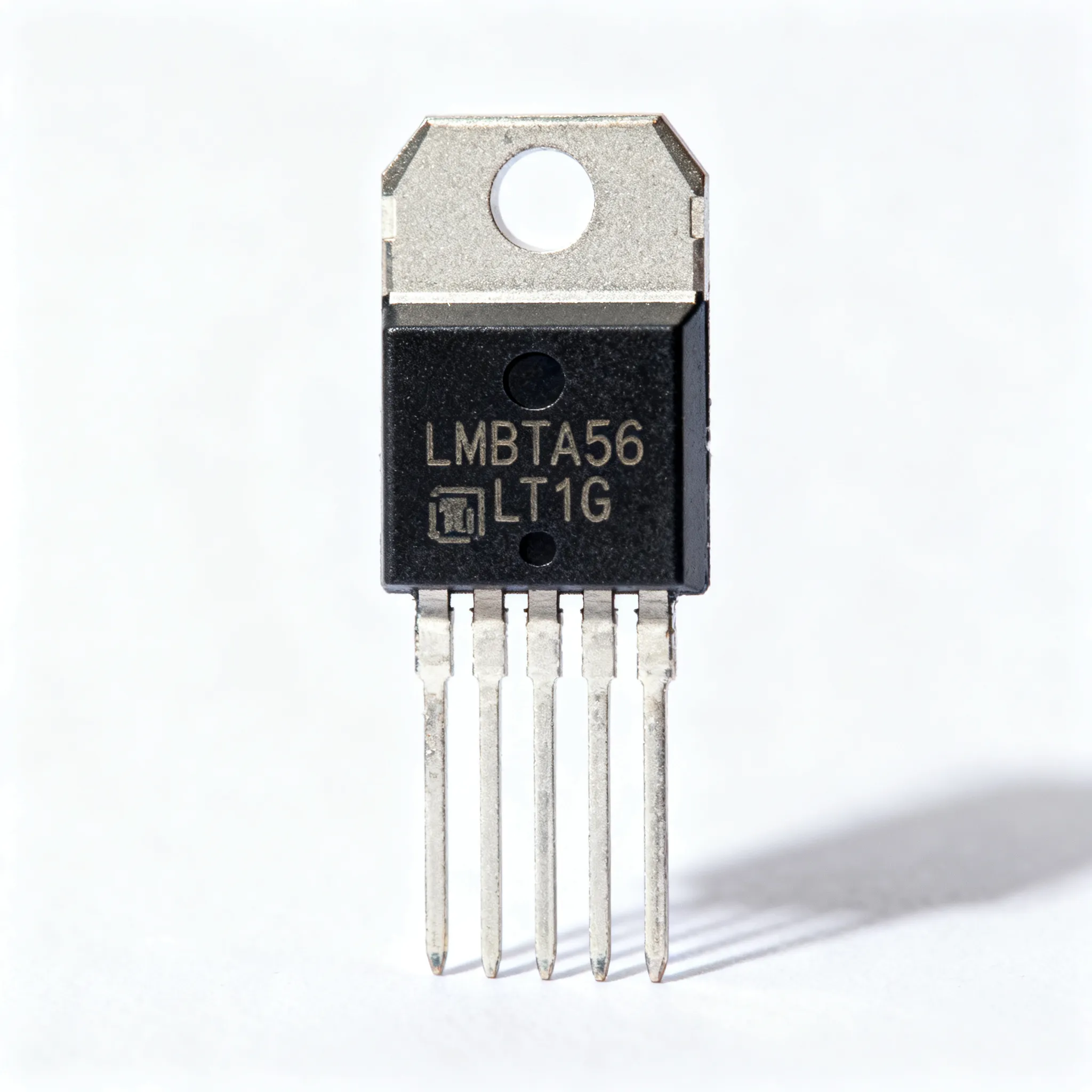
Commodity small-signal transistors rarely make headlines, yet they can stall a production line just as effectively as a high-end microcontroller. The lead time for a single SOT-23 PNP device can stretch to several months when allocation tightens, and procurement teams running high-volume builds cannot afford to wait. The LMBTA56LT1G—an 80 V, 500 mA PNP bipolar transistor from Onsemi in a three‑lead SOT‑23 package—sits squarely in that risk zone. Although it is a mature, widely used part, single‑source BOMs expose you to price spikes and delivery gaps the moment fab capacity shifts.
Recent industry data confirms that pin‑compatible replacements can cut lead times by 40–60 % while delivering measurable cost savings source. That statistic isn’t limited to analog ICs; it applies equally to commodity discretes. For the LMBTA56LT1G, the most immediate alternative is the MMBTA56-7-F from Diodes Incorporated, which shares the same footprint and key electrical ratings. A systematic cross‑reference exercise—backed by datasheet evidence and verified supply‑chain data—is what separates a reactive BOM change from a deliberate, cost‑optimized sourcing strategy. The following sections walk you through the device fundamentals, compare the primary drop‑in candidates, and lay out a practical qualification workflow that keeps quality intact while you regain control of lead times and budget.
Understanding the LMBTA56LT1G: Key BJT Parameters and Thermal Limits
Before you can evaluate any alternative, you need a clear picture of what the LMBTA56LT1G actually delivers. This is a PNP bipolar junction transistor fabricated on a silicon planar process, rated for maximum collector‑emitter voltage (VCEO) of 80 V and continuous collector current (IC) of 500 mA. Total power dissipation is specified at 225 mW when mounted on a standard FR‑4 board with minimum copper area, and the junction can operate from −55 °C to +150 °C sourcesource. The DC current gain (hFE) is typically 100 at a collector current of 100 mA and a collector‑emitter voltage of 1 V, while the transition frequency (fT) sits at 50 MHz, making the device suitable for general‑purpose amplification and moderate‑speed switching.
One point that often causes confusion: the die inside LMBTA56LT1G is identical to the one used in the MMBTA56LT1G. The “L” prefix denotes a lead‑free, RoHS‑compliant finish; the SMD marking “2GM” is the same on both. If your assembly process is RoHS‑compliant, either version works, but the BOM must reflect the correct suffix to avoid incoming‑inspection hiccups. The table below summarizes the critical parameters you need to pin down before any substitution.
| Parameter | Value | Unit / Condition |
|---|---|---|
| Collector‑Emitter Voltage (VCEO) | 80 | V |
| Collector‑Base Voltage (VCBO) | 80 | V |
| Emitter‑Base Voltage (VEBO) | 4 | V |
| Continuous Collector Current (IC) | 500 | mA |
| Power Dissipation (PD) | 225 | mW (FR‑4, min. Cu) |
| DC Current Gain (hFE) | 100 (typ.) | @ IC = 100 mA, VCE = 1 V |
| Transition Frequency (fT) | 50 | MHz |
| Collector‑Emitter Saturation Voltage (VCE(sat)) | 250 | mV (max) @ IC = 500 mA, IB = 50 mA |
| Package | SOT‑23 | 3‑lead plastic |
| Junction Temperature Range | −55 to +150 | °C |
Tip: When you are reviewing an alternative datasheet, start with the absolute maximum ratings and the hFE curves at the specific collector current your circuit draws. A 500 mA rating alone doesn’t guarantee the gain stays above your minimum requirement at the operating point.
MMBTA56LT1G vs. MMBTA56-7-F and Other Pin-Compatible Replacements
The two most practical drop‑in candidates for the LMBTA56LT1G are the Onsemi MMBTA56LT1G (the base part number) and the Diodes Incorporated MMBTA56-7-F. Both come in a standard SOT‑23 outline, share the same pinout (Base‑Emitter‑Collector looking at the flat face), and are rated for 80 V VCEO and 500 mA IC. The Ovaga Technologies comparison source confirms that physical footprint and core electrical ratings are equivalent, but subtle differences in power dissipation, saturation voltage, and gain binning can affect circuit behaviour in marginal designs.
Nexperia’s alternative selection guide source and the NTE Semiconductor Technical Guide source offer additional paths to identify functionally equivalent parts, but neither provides a direct SOT‑23 80 V PNP transistor with an identical pin‑for‑pin match. The Nexperia portfolio includes devices like the BC856 (65 V) and PMBT4403 (40 V) that approach the voltage and current range, but they require a pin‑out change and a full re‑validation. For most high‑volume production lines, the MMBTA56-7-F remains the most straightforward path to a cost‑optimized second source.
The comparison matrix below highlights the key parameters side by side, with selection notes that help you decide when a parameter difference is acceptable and when it demands caution.
| Parameter | LMBTA56LT1G (Onsemi) | MMBTA56-7-F (Diodes Inc.) | Selection Criteria & Failure Boundary |
|---|---|---|---|
| VCEO | 80 V | 80 V | Identical. No margin concern. |
| IC (continuous) | 500 mA | 500 mA | Identical. Verify PCB trace and derating. |
| PD (total dissipation) | 225 mW | 300 mW | Diodes part offers 33 % higher thermal headroom; beneficial in cramped layouts. |
| hFE at 100 mA | 100 (typ.) | 100 (typ.) | Typical values match. Min/max bins may differ—check the P/N suffix for gain group. |
| VCE(sat) max at 500 mA | 250 mV | 250 mV | Identical max limit. Diodes datasheet often shows typical 90 mV; Onsemi typical 100 mV. Confirm in your switching circuit. |
| fT | 50 MHz | 50 MHz | No difference for general‑purpose or audio‑band circuits. |
| Package / Pinout | SOT‑23 (B‑E‑C) | SOT‑23 (B‑E‑C) | Drop‑in compatible. No layout change required. |
| Typical lead time (2025) | 12–16 weeks | 4–8 weeks | 40–60 % shorter source; confirm with your distributor. |
The higher power dissipation rating of the MMBTA56-7-F is a real advantage in designs where the transistor runs near the 225 mW limit. However, the gain group suffix (e.g., -7-F vs. -13-F) can influence the minimum hFE at low collector currents. Always request the full datasheet and, if possible, the qualification test report before committing to a production‑volume switch.
Sourcing Smart: How to Evaluate Cost-Optimized Replacements Without Compromising Quality
A successful BOM substitution starts well before the first purchase order. The TI alternatives guide source underscores that physical compatibility does not guarantee electrical or thermal match, and the same principle holds when you are swapping a mature PNP transistor. The following steps, drawn from the PCBA risk‑management approach described in the alternative electronic components guide, form a repeatable workflow:
- Compare datasheets parameter‑by‑parameter. Look beyond the headline numbers: examine the gain vs. collector current curves, the saturation voltage profiles, and the SOA (Safe Operating Area) charts. Even a small increase in VCE(sat) can increase power dissipation in a low‑side switch.
- Verify package thermal resistance. The Diodes MMBTA56-7-F may dissipate 300 mW, but its junction‑to‑ambient thermal resistance θJA is roughly 417 °C/W on a 1‑inch² copper pad. Compare that with the Onsemi value of 556 °C/W for the LMBTA56LT1G. The better thermal path can lower junction temperature under the same load, improving reliability.
- Request qualification samples. A 10‑piece bench test is not enough. Ask your distributor for a reel from the same date code you would receive in production and run the alternative through worst‑case operating conditions: minimum supply voltage, maximum ambient temperature, and maximum collector current.
- Test in‑circuit with a representative PCB. Solder the sample onto the exact board layout and verify switching waveforms, rise/fall times, and any oscillation tendencies. The 50 MHz fT of both parts is benign, but parasitic layout differences can interact with the transistor’s Miller capacitance.
- Source only from authorized distributors. Counterfeit small‑signal transistors are a well‑known problem. Stick to franchised sources such as Arrow source or Digi‑Key, and insist on traceability documentation.
- Validate the second source with a pilot build. Run a few hundred boards through the normal assembly and test flow. Monitor the first‑pass yield and any parametric shifts at final test. This step catches subtle issues like changed turn‑on time that a bench test might miss.
The table below summarizes the most important parameters to verify and the acceptable tolerance window when substituting a small‑signal PNP transistor in a high‑volume production environment.
| Parameter | Tolerance Window | Verification Method | Risk if Mismatch |
|---|---|---|---|
| VCEO | ≥80 V | Curve tracer, breakdown test | Catastrophic failure on overvoltage |
| IC (continuous) | ≥500 mA | DC load test at max. temp. | Thermal runaway, reduced lifetime |
| PD | ≥225 mW | Thermal imaging, θJA calculation | Junction overheat, derating violation |
| hFE at operating IC | Within ±20 % of baseline | Semiconductor parameter analyser | Insufficient drive, saturation |
| VCE(sat) at IC(max) | ≤250 mV | Pulsed measurement, low duty cycle | Excess power dissipation, heating |
| fT | ≥40 MHz | Network analyser, s‑parameter | Reduced bandwidth, oscillation |
| Pinout | B‑E‑C (SOT‑23) | Visual inspection, continuity | Board damage, incorrect bias |
Note: The Nexperia alternative selection guide source reinforces that a parameter‑by‑parameter comparison is essential. Even a part that looks identical on paper may behave differently at the corners of its operating envelope. Don’t skip the in‑circuit validation step—it’s the cheapest insurance against a field return.
LMBTA56LT1G Procurement Q&A: What Engineers and Buyers Are Asking
Senior engineers and procurement leads often converge on the same six questions when evaluating a second source for the LMBTA56LT1G. The answers below are grounded in the datasheet evidence and supply‑chain data referenced throughout this guide.
Q: What is the difference between LMBTA56LT1G and MMBTA56LT1G?
They are electrically identical—the ‘L’ prefix indicates a lead‑free, RoHS‑compliant version. Both use the same SOT‑23 die and carry the same marking ‘2GM’. The MMBTA56LT1G is the base part number; either can be used as long as the bill of materials reflects the correct suffix for your assembly process.
Q: Is the MMBTA56-7-F a direct drop‑in replacement for LMBTA56LT1G?
Yes, in most applications. Pinout, SOT‑23 footprint, and key ratings (VCEO = 80 V, IC = 500 mA) match. However, compare VCE(sat) and hFE min/max bins from the Diodes Inc. datasheet source, and verify thermal performance in your circuit before full production. The Diodes part’s higher power dissipation rating (300 mW) can be a benefit, but the gain group suffix may affect low‑current behaviour.
Q: How can I secure long‑term availability when switching to an alternative?
Source from authorized distributors, check the manufacturer’s lifecycle status and PCN history, and consider qualifying a second source with a similar footprint. The TI alternatives guide source highlights that multi‑sourcing can cut lead times by 40–60 % and reduce price volatility. For the LMBTA56LT1G, maintaining a qualified vendor list that includes both Onsemi and Diodes Incorporated is a low‑effort way to insulate your BOM.
Q: What are the critical parameters to verify when cross‑referencing small‑signal PNP transistors?
Match VCEO, IC, PD, and package first. Then check hFE at the operating current, fT for speed‑dependent circuits, and VCE(sat) for low‑side switching. The Nexperia alternative selection guide source reinforces that a parameter‑by‑parameter comparison is essential to avoid functional failures. Don’t ignore the Safe Operating Area (SOA) curve, especially if the transistor sees inductive loads.
Q: Are there Nexperia devices that can replace the LMBTA56LT1G?
Nexperia does not have a direct footprint equivalent for the 80 V PNP SOT‑23 LMBTA56LT1G. However, their cross‑reference tool source can identify similar voltage/current parts in the BC856 or PMBT4403 families, though these often require pin‑out adjustment and re‑validation. The MMBTA56-7-F remains the most straightforward drop‑in.
Q: What is the typical lead time for LMBTA56LT1G and its alternatives?
Onsemi’s lead time for the LMBTA56LT1G can extend to 12–16 weeks during allocation periods. Diodes Inc. alternatives like the MMBTA56-7-F are frequently available in 4–8 weeks, consistent with the 40–60 % lead‑time reduction observed across pin‑compatible replacements source, though actual lead times depend on volume and market conditions. Always confirm with your distributor and consider buffer stock of the alternative to cover the qualification period.
References & Further Reading
- LMBTA56LT1G Datasheet and Replacement, Transistor Equivalent Finder – AllTransistors.com
- MMBTA56LT1G – onsemi Bipolar (BJT) – JLCPCB
- MMBTA56LT1G and MMBTA56-7-F Specification Comparison – Ovaga Technologies
- Nexperia Chip Alternative Selection Guide – Utmel
- TI Chip Alternatives 2025: Pin-Compatible Replacements Guide – Hitop-Tech
- Alternative Electronic Components for Safer PCBA Builds – BestPCBs
- NTE Semiconductor Technical Guide and Cross Reference – Datasheet Archive
- MMBTA56LT1G by onsemi – Arrow