MBR30150CT Datasheet and Pinout: Specs for Design and Sourcing
MBR30150CT datasheet essentials, pinout overview, key specs, and design/sourcing checks for engineers and buyers. Request a quote on IC-Online.
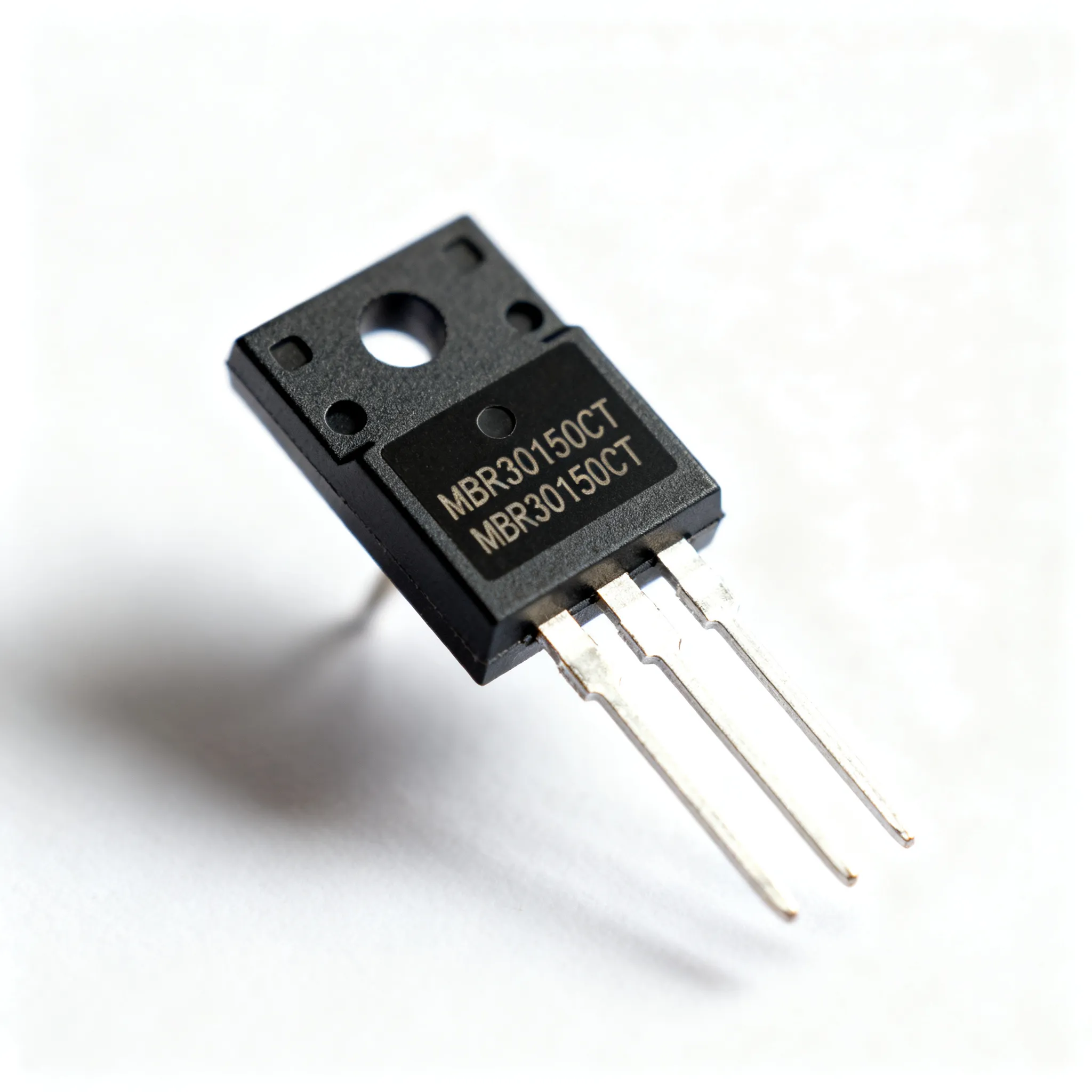
When you're laying out a high‑current power converter — whether it's an industrial AC‑DC front end, a server redundant‑rail OR‑ing stage, or a telecom rectifier pushing 25 A continuous — the rectifier you specify determines far more than just conduction loss. It shapes your thermal budget, your PCB footprint, and increasingly, your procurement timeline. The MBR30150CT has earned its place in these designs through a combination of rugged 150 V Schottky barrier technology, a dual common‑cathode configuration that simplifies high‑side rectification, and a TO‑220 package that most power engineers can rout in their sleep. This article is a deep‑dive into the datasheet essentials, pinout details, and real‑world design constraints that matter when you're integrating this 30 A dual rectifier into a high‑efficiency power stage — and how to approach sourcing it without falling into allocation traps that have plagued commodity semiconductors.
Why the MBR30150CT Remains a Go‑To Dual Schottky Rectifier in Tight Supply Chains
Power rectifiers occupy a strange middle ground in component procurement. They are simultaneously commodity parts — manufactured in high volume across multiple fabs — and specialty devices whose surge ratings, thermal impedance, and reverse leakage behaviour are tightly coupled to a specific manufacturer's process. The MBR30150CT exemplifies this duality. On paper, it's a straightforward 2×15 A, 150 V dual Schottky in a TO‑220‑3 package. In practice, its low forward voltage drop (typically 0.75 V at 15 A per leg, Tj = 125 °C) and rugged avalanche capability have made it a default choice in secondary‑side rectification for LLC and phase‑shifted full‑bridge converters operating in the 100–300 kHz range.
What makes a well‑understood part like this strategically valuable today isn't novelty — it's predictability. As EE Times has documented extensively through 2024 and early 2025, semiconductor allocation pressures have shifted unpredictably across device categories. Power discretes, once considered immune to the shortages that hit MCUs and FPGAs, faced their own capacity constraints as fabs rebalanced wafer starts toward higher‑margin logic and memory products. A rectifier with mature process stability, multi‑source packaging infrastructure, and a deep paper trail of reliability data reduces the engineering time spent re‑qualifying alternatives mid‑design. That predictability translates directly to BOM stability — something every procurement manager values when lead‑time uncertainty persists across the broader semiconductor landscape.
Key Takeaway: The MBR30150CT isn't the newest Schottky on the market, but it's one of the most thoroughly characterized. In an era where re‑qualification costs can exceed the per‑unit savings of a substitute part, choosing a rectifier with decades of field history and clear sourcing documentation is a prudent engineering decision, not a conservative one.
Inside the Datasheet: Decoding 30 A, 150 V Dual Common‑Cathode Specs and Pinout
The MBR30150CT package is a three‑terminal TO‑220‑3 (also available in TO‑247 for higher thermal mass applications), and understanding the pinout is step one for any layout engineer. The central terminal — the tab — serves as the common cathode connecting both internal Schottky dies. The two outer pins (pins 1 and 3) are the independent anodes. This common‑cathode topology is purpose‑built for positive‑output rectification: both anodes receive AC from a center‑tapped transformer or full‑bridge secondary, while the cathode delivers the rectified DC output to the output filter. It's a configuration that eliminates the need for separate diode packages in dual‑rail designs and reduces parasitic inductance compared to paralleling two discrete TO‑220 single Schottkys.
From a datasheet perspective, the numbers engineers need to internalize fall into three categories: static conduction parameters, dynamic switching and surge limits, and thermal boundary conditions. The table below extracts the Tier‑A specifications you'll reference repeatedly during design validation.
| Parameter | Value | Conditions / Notes |
|---|---|---|
| Maximum Repetitive Peak Reverse Voltage (VRRM) | 150 V | Per leg; applies across full TJ range |
| Average Forward Current (IO) | 30 A total (15 A per leg) | TC = 125 °C; both legs conducting |
| Peak Forward Surge Current (IFSM) | 250 A | 8.3 ms single half‑sine, TJ = 25 °C |
| Forward Voltage (VF) | 0.75 V typ. per leg | IF = 15 A, TJ = 125 °C |
| Forward Voltage (VF) at 25 °C | 0.92 V max. per leg | IF = 15 A, TJ = 25 °C |
| Peak Repetitive Reverse Current (IRRM) | 0.5 mA typ., 50 mA max. | VR = 150 V, TJ = 125 °C |
| Junction Capacitance (CJ) | 500 pF typ. per leg | VR = 5 V, f = 1 MHz |
| Junction Temperature Range (TJ) | −55 to +150 °C | Exceeding 150 °C risks thermal runaway |
| Thermal Resistance, Junction‑to‑Case (RθJC) | 1.5 °C/W per leg | TO‑220; both legs share the tab |
| Thermal Resistance, Junction‑to‑Ambient (RθJA) | 60 °C/W | No heatsink; natural convection |
| Package | TO‑220‑3 (TO‑247 optional) | Common cathode on tab (pin 2) |
Pinout Detail: Common Cathode on the Tab
Pin identification for the MBR30150CT in the TO‑220‑3 package follows a consistent convention: pin 1 is anode 1 (leftmost when viewing the front, marking side), pin 2 is the common cathode (electrically connected to the metal tab), and pin 3 is anode 2 (rightmost). In many PCB layouts, the tab is bolted directly to a heatsink that may be grounded or floating. Engineers must ensure that if the heatsink is grounded and the cathode is at a positive output potential, an insulating pad and bushings are used — otherwise, a direct short to ground results. The TO‑247 variant offers a larger thermal pad and is preferred when sustained operation above 20 A total output is expected, though the electrical pinout remains identical.
Tip: Always verify the tab potential in your circuit before finalizing mechanical assembly. The common‑cathode‑on‑tab design is convenient for positive‑output rectifiers but creates a safety hazard if the heatsink is exposed and the cathode sits at 48 V or higher. Use a Sil‑Pad or mica insulator with thermal grease rated for your maximum TC.
One nuance often overlooked in datasheet reviews: at TJ = 25 °C, the maximum forward voltage is specified at 0.92 V per leg, but at elevated junction temperatures (125 °C), the forward voltage drops to approximately 0.75 V typical. This negative temperature coefficient of VF is characteristic of Schottky barriers and benefits efficiency at high load. However, it demands careful thermal design — a hotter junction conducts more current, which produces more heat — and without adequate heatsinking, this feedback loop can accelerate toward thermal runaway. More on mitigating this risk in the thermal design section below.
MBR30150CT vs. Competing 150 V Dual Schottkys: Performance and Package Trade‑offs
No rectifier exists in isolation, and design teams evaluating the MBR30150CT typically compare it against two or three alternatives that occupy the same 150 V, TO‑220, dual‑Schottky niche. The most common references are the STPS30H150CT from STMicroelectronics and the MBR20150CT (a 20 A sibling in the same product family). Each brings a slightly different balance of forward voltage, reverse leakage, and thermal resistance to the table. The comparison below is grounded in publicly available datasheet parameters and should inform your selection — but final validation must always be performed with your specific operating conditions, including switching frequency, di/dt, and ambient temperature envelope.
| Comparison Metric | MBR30150CT (onsemi / equivalent) | STPS30H150CT (STMicroelectronics) | MBR20150CT (20 A sibling) | Selection Criteria & Failure Boundary |
|---|---|---|---|---|
| VRRM | 150 V | 150 V | 150 V | Equal rating; verify derating for 80% of VRRM in continuous operation |
| IO (total, per device) | 30 A (2×15 A) | 30 A (2×15 A) | 20 A (2×10 A) | MBR20150CT suits sub‑15 A total designs; 30 A parts provide headroom for load transients |
| VF typ. @ 15 A, 125 °C | 0.75 V | 0.78 V | 0.80 V @ 10 A, 125 °C | 30 mV difference equates to ~0.9 W less dissipation at 30 A total; evaluate in full thermal context |
| IFSM (8.3 ms surge) | 250 A | 220 A | 180 A | Higher surge rating provides margin for inrush and fault conditions; verify with actual bus capacitance |
| RθJC per leg | 1.5 °C/W | 1.2 °C/W | 1.8 °C/W | STPS30H150CT's lower RθJC may allow smaller heatsink; verify mounting torque specs differ |
| IR max. @ 150 V, 125 °C | 50 mA | 60 mA | 25 mA | Leakage directly impacts light‑load efficiency; the 20 A part leaks less but at reduced current capacity |
| Package options | TO‑220, TO‑247 | TO‑220, D²PAK, TO‑247 | TO‑220, TO‑247 | STPS30H150CT's SMD D²PAK option suits automated assembly; verify pad layout for thermal vias |
Several observations emerge from this comparison. First, the STPS30H150CT offers a marginally lower thermal resistance (1.2 °C/W vs. 1.5 °C/W per leg), which can translate to a 2–3 °C lower junction temperature at full load — meaningful if your ambient is already at 85 °C and every degree eats into your reliability margin. The trade‑off is slightly higher reverse leakage at the maximum rated voltage and temperature (60 mA vs. 50 mA), which may impact standby power consumption in always‑on designs. Footnote for design teams: both the MBR30150CT and STPS30H150CT require verification of gate‑drive timing and snubber network values in the target converter. Surge ratings and dynamic VF behaviour during commutation are not identical, and a direct swap without re‑testing can lead to unexpected voltage overshoot on the secondary side.
The MBR20150CT, while pin‑compatible, is a 20 A part and should only be considered if the application's continuous output current remains below approximately 14 A total (with a conservative derating factor). Attempting to push 25 A through a 20 A‑rated rectifier — even with exceptional cooling — exceeds the manufacturer's absolute maximum ratings and voids any reliability guarantees. Use the 20 A variant for lower‑power designs where its reduced leakage (25 mA at 150 V, 125 °C) benefits standby efficiency.
Important: None of these alternatives should be dropped into a BOM without verifying surge rating adequacy, pinout compatibility (all three share the same TO‑220 common‑cathode assignment), and thermal pad electrical connectivity. Evaluate substitutions as candidates requiring full validation, not as guaranteed drop‑ins.
Designing Reliable Power Stages with the MBR30150CT: Thermal, Layout, and Procurement Priorities
The gap between a datasheet‑perfect simulation and a field‑reliable power supply often comes down to three things: how well you manage heat, how carefully you rout the high‑current loops, and how thoroughly you vet your supply chain. When integrating the MBR30150CT into a power stage, treat thermal design as a first‑order electrical constraint, not a mechanical afterthought.
Thermal Management: Heatsink Sizing and Derating
At a continuous output current of 25 A total (12.5 A per leg), with a typical forward voltage of 0.80 V at TJ ≈ 100 °C, each leg dissipates roughly 10 W. Total device dissipation approaches 20 W. Using the junction‑to‑case thermal resistance of 1.5 °C/W per leg, the junction temperature rise above the case is approximately 15 °C per leg — but because both dies share the same tab, the effective RθJC for total power dissipation is lower (around 0.75 °C/W for the package as a whole). The case temperature must therefore be kept below approximately 115 °C to maintain TJ under the 150 °C absolute maximum, assuming worst‑case VF and some margin for transient overloads.
| Thermal Design Parameter | Recommended Value / Range | Derating Guidance |
|---|---|---|
| Maximum TJ for continuous operation | 125 °C (derated from 150 °C abs. max.) | 25 °C margin accounts for transient overload and aging |
| Heatsink RθSA for 25 A, 40 °C ambient | < 2.5 °C/W (natural convection) | Forced air at 200 LFM reduces heatsink requirement to ~3.5 °C/W |
| Thermal interface material | Silicone‑based pad, RθCS < 0.5 °C/W | Avoid dry mounting; use calibrated torque (0.5–0.8 N·m for TO‑220) |
| Maximum PCB lead length to heatsink | < 15 mm | Longer leads increase RθJA and introduce parasitic inductance in the commutation loop |
| Thermal vias under TO‑220 tab (if SMD variant used) | ≥ 9 vias, 0.3 mm diameter, plugged with epoxy or solder mask | Vias improve heat spreading to bottom‑side copper pour; IPC‑A‑610 Class 2 solderability applies |
| Derating above TC = 100 °C | Reduce IO by 1.5% per °C above 100 °C | Linear derating; at TC = 125 °C, maximum IO ≤ 18 A total |
| Parallel operation | Not recommended without current‑sharing resistors (≤ 10 mΩ each leg) | Negative VF temperature coefficient causes current hogging in direct parallel |
Layout and Assembly Best Practices
Power PCB layout for the MBR30150CT revolves around minimizing the high‑frequency commutation loop area. The AC connections from the transformer secondary to the two anodes (pins 1 and 3) and the return path from the cathode (pin 2 / tab) to the output filter capacitor should form the smallest possible physical loop. Wide copper pours — at least 8 mm for 15 A continuous — keep trace heating manageable and reduce parasitic inductance that exacerbates ringing at turn‑off.
Soldering practices should align with IPC‑A‑610 Class 2 acceptability standards as a minimum; Class 3 is advisable for mission‑critical industrial or medical applications. The TO‑220 leads demand through‑hole wave or selective soldering with a dwell time not exceeding 5 seconds at 260 °C. Excessive soldering duration can delaminate the internal bond wires, particularly if the device has been stored in a humid environment without pre‑baking. For volume production, pin‑in‑paste reflow with proper stencil aperture design can yield consistent joints without the thermal shock of wave soldering.
Warning on parallel operation: Connecting both anodes together to create a single 30 A diode is a common but risky practice. The two internal Schottky dies are not perfectly matched, and their negative VF temperature coefficient means that whichever die runs slightly hotter will draw more current — heating further and eventually taking a disproportionate share of the total load. If you must parallel, add external ballast resistors (5–10 mΩ, rated for at least 2 W) in series with each anode to improve current sharing. Even then, treat the combined assembly as a 25 A device, not 30 A, to allow for imbalance.
MBR30150CT Sourcing and Application Q&A
The questions below reflect real conversations that engineers and purchasing teams have when the MBR30150CT appears on a BOM — from variant confusion to counterfeit detection to thermal boundary conditions that datasheet charts don't always make explicit. Use these answers as a starting point for discussions with your authorized distributor or contract manufacturer.
Q: What distinguishes the MBR30150CT from the MBR30150CT‑1 or MBR30150CT‑G variants?
Differences between the base MBR30150CT and its suffix variants are typically limited to lead‑finish composition (lead‑free / RoHS compliance) and packaging format (bulk vs. tube/rail). The MBR30150CT‑G designation usually indicates a halogen‑free, RoHS‑compliant version with matte‑tin leads. The MBR30150CT‑1 may refer to a specific packing quantity or reel configuration. Electrical specifications — forward voltage, reverse leakage, surge current, and thermal resistance — are identical across these variants. Always verify the suffix meaning on the manufacturer's original datasheet addendum or packaging information document, as suffix conventions vary between onsemi, Lite‑On, and other licensed manufacturers of this part number.
Q: Can I replace a single 30 A Schottky with one‑half of the MBR30150CT by leaving the second anode open?
Yes, you can use only one leg of the MBR30150CT by leaving the unused anode pin floating, but two important derating rules apply. First, the continuous current rating for a single leg is 15 A, not 30 A — the 30 A rating assumes both legs conduct equally. Second, thermal performance changes: with only one die active, heat still spreads through the entire package and tab, but the hotspot is concentrated over one corner of the die‑attach pad. The effective RθJC for single‑leg operation is approximately 2.0 °C/W (worse than the 1.5 °C/W per‑leg spec when both legs are active). Treat the part as a 15 A single Schottky with a larger case footprint, and size your heatsink accordingly. If your design truly needs only 15 A capability, the MBR20150CT or a single‑die 15 A Schottky may be more cost‑effective and thermally predictable.
Q: What is a realistic heatsink requirement for 25 A continuous output in a 100 °C ambient?
This is a demanding thermal scenario. At 25 A total (12.5 A per leg) and TJ of approximately 125 °C, each leg's VF is roughly 0.78 V, giving per‑leg dissipation of 9.75 W — approximately 19.5 W total for the device. With an effective package RθJC of ~0.75 °C/W (both legs active), the case temperature must stay below 125 °C − (19.5 × 0.75) = 110 °C. The heatsink must then dissipate 19.5 W from 110 °C case to 100 °C ambient — a mere 10 °C rise — meaning the heatsink thermal resistance RθSA must be less than 0.51 °C/W. This is well below what passive natural‑convection heatsinks can achieve in a reasonable volume. Forced‑air cooling is therefore mandatory in this scenario; a heatsink rated at 0.8 °C/W with 200–400 LFM airflow can maintain safe junction temperatures. If forced air is unavailable, consider a TO‑247 package variant with a larger thermal interface, or reduce the per‑device current by paralleling two rectifiers with external ballast resistors. Always confirm your thermal calculations with thermocouple measurements on a prototype under worst‑case load and ambient conditions.
Q: How do I detect and avoid counterfeit MBR30150CT parts?
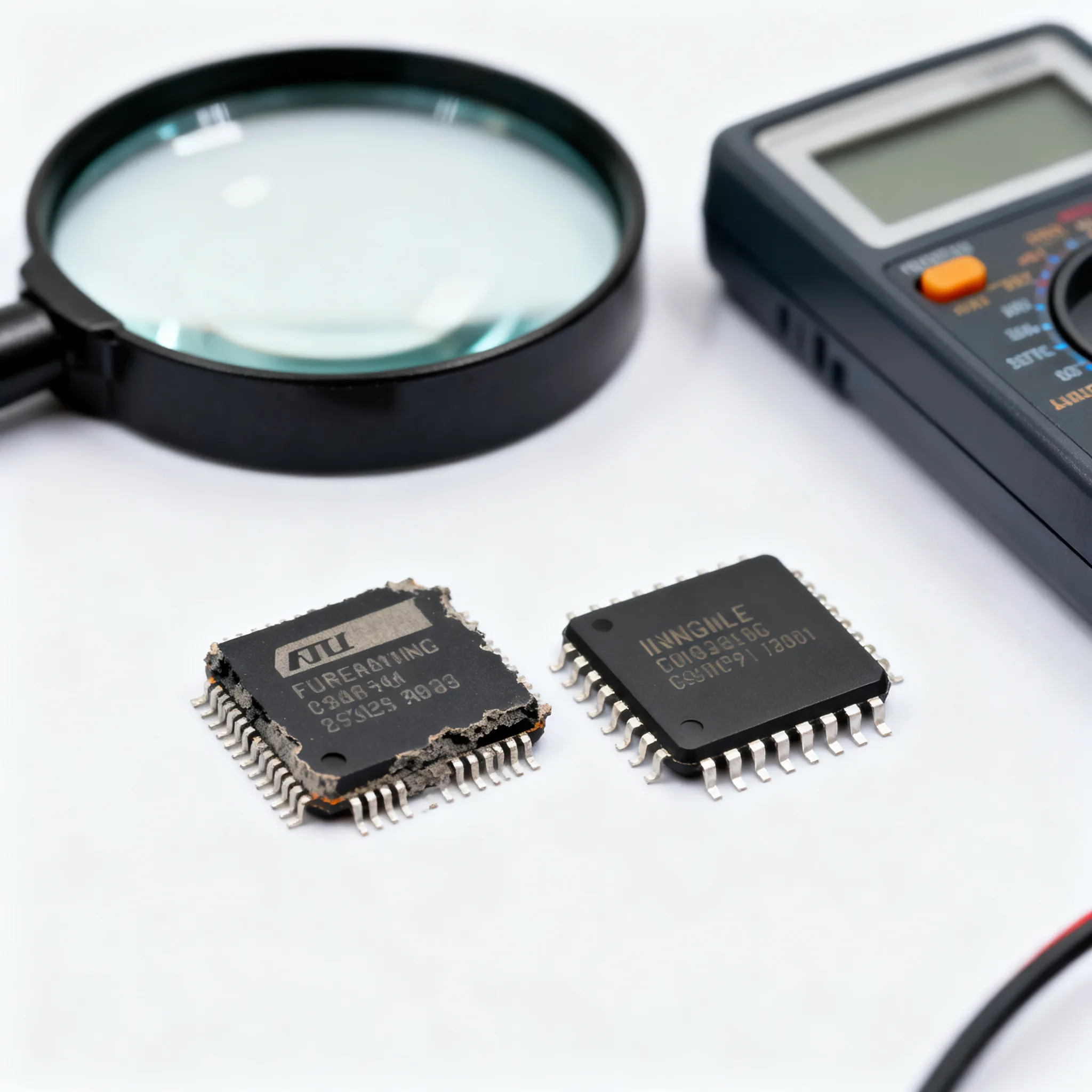
Counterfeit Schottky rectifiers continue to circulate in non‑franchised distribution channels, and the MBR30150CT is no exception. Red flags include laser marking that appears shallow or etched rather than deeply engraved (genuine parts from major manufacturers use consistent marking depth and font), absence of a legible batch code or date code, and forward voltage measurements that deviate significantly from the datasheet envelope — particularly at low forward current (e.g., VF > 0.4 V at IF = 1 A at room temperature). Genuine Schottky junctions exhibit a characteristic logarithmic I‑V relationship; counterfeits — often remarked commodity PN‑junction diodes — show a sharper knee voltage and higher forward drop at low currents.
Procurement teams should require the following from suppliers when sourcing this part: (a) a valid certificate of conformance tracing the lot to the original manufacturer, (b) date codes no older than 24 months from the date of shipment, and (c) X‑ray inspection reports if the supply chain includes non‑franchised intermediaries. X‑ray imaging reveals internal die size and bond‑wire count, which can be compared against a known‑genuine reference sample. Above all, purchasing through authorized distributor networks — even if the unit price is modestly higher — is the most effective counterfeit mitigation strategy for a production BOM. Request a sample batch and perform electrical characterization across temperature before committing to a volume order from an unfamiliar source.
Q: Why does reverse leakage increase dramatically at the upper temperature limit?
Schottky barrier diodes exhibit a strong positive temperature coefficient of reverse leakage current — a fundamental property of the metal‑semiconductor junction. At TJ = 25 °C, reverse leakage for the MBR30150CT is typically under 100 µA at VR = 150 V. At TJ = 150 °C, leakage can exceed 50 mA per leg — a more than 500‑fold increase. This leakage current flows even when the diode is reverse‑biased, contributing to power dissipation that must be accounted for in light‑load and standby conditions.
The design implications are most acute in discontinuous‑conduction‑mode (DCM) flyback and resonant converters, where the rectifier experiences the full reverse voltage for a significant portion of each switching cycle. At high ambient temperatures, the additional 50–100 mA of leakage per leg (depending on the exact junction temperature and reverse voltage) can push standby power consumption beyond regulatory limits such as Energy Star or EU Ecodesign Tier 2. Mitigation strategies include specifying a heatsink that maintains TJ below 125 °C even under worst‑case ambient, using a synchronous rectifier (MOSFET) for the low‑side position where conduction and leakage losses are highest in DCM, or selecting an alternative Schottky with lower specified leakage at elevated temperature — at the cost of slightly higher forward voltage. Datasheet leakage curves (IR vs. TJ at fixed VR) are essential design inputs; do not rely solely on the 25 °C leakage specification when evaluating thermal budget.
After evaluating these application and sourcing considerations, design teams should have a clear picture of where the MBR30150CT fits — and where it doesn't. The part excels in high‑current, high‑ambient applications where its rugged surge rating and mature packaging infrastructure offset slightly higher forward losses compared to newer silicon‑carbide alternatives. For designs pushing the boundaries of density and efficiency above 94%, a SiC Schottky may be worth the cost premium; for the vast majority of industrial and telecom rectification tasks, this dual 150 V Schottky remains the pragmatic choice.
References & Further Reading
- onsemi — Discrete & Power Solutions — Manufacturer datasheets and application notes for Schottky rectifiers including the MBR30150CT family.
- STMicroelectronics — STPS30H150CT Product Page — Comparative datasheet for the competing 30 A, 150 V dual Schottky in TO‑220.
- EE Times — Electronics Engineering News & Analysis — Coverage of semiconductor supply chain dynamics, allocation trends, and power discretes market analysis.
- IPC — IPC‑A‑610 Acceptability of Electronic Assemblies — Soldering workmanship standards applicable to through‑hole power components including TO‑220 packages.
- Digi‑Key Electronics — Engineering resources, datasheet downloads, and parametric search tools for Schottky rectifiers and thermal management components.
- Mouser Electronics — Component distributor with technical documentation and thermal design resources for power semiconductors.
- IC-Online — Electronic Component Sourcing Platform — RFQ and BOM upload for the MBR30150CT and related power discretes; mixed‑BOM procurement with flexible MOQ.
- Semiconductor Industry Association (SIA) — Industry data and policy analysis on semiconductor manufacturing capacity and trade.
Ready to integrate the MBR30150CT into your next power design? Whether you're sourcing prototypes for validation or negotiating volume pricing for production, the IC-Online platform connects you with verified suppliers who understand the requirements of high‑reliability power discretes. Request a quote or upload your BOM now — flexible minimum order quantities and cross‑referencing support for your full bill of materials.