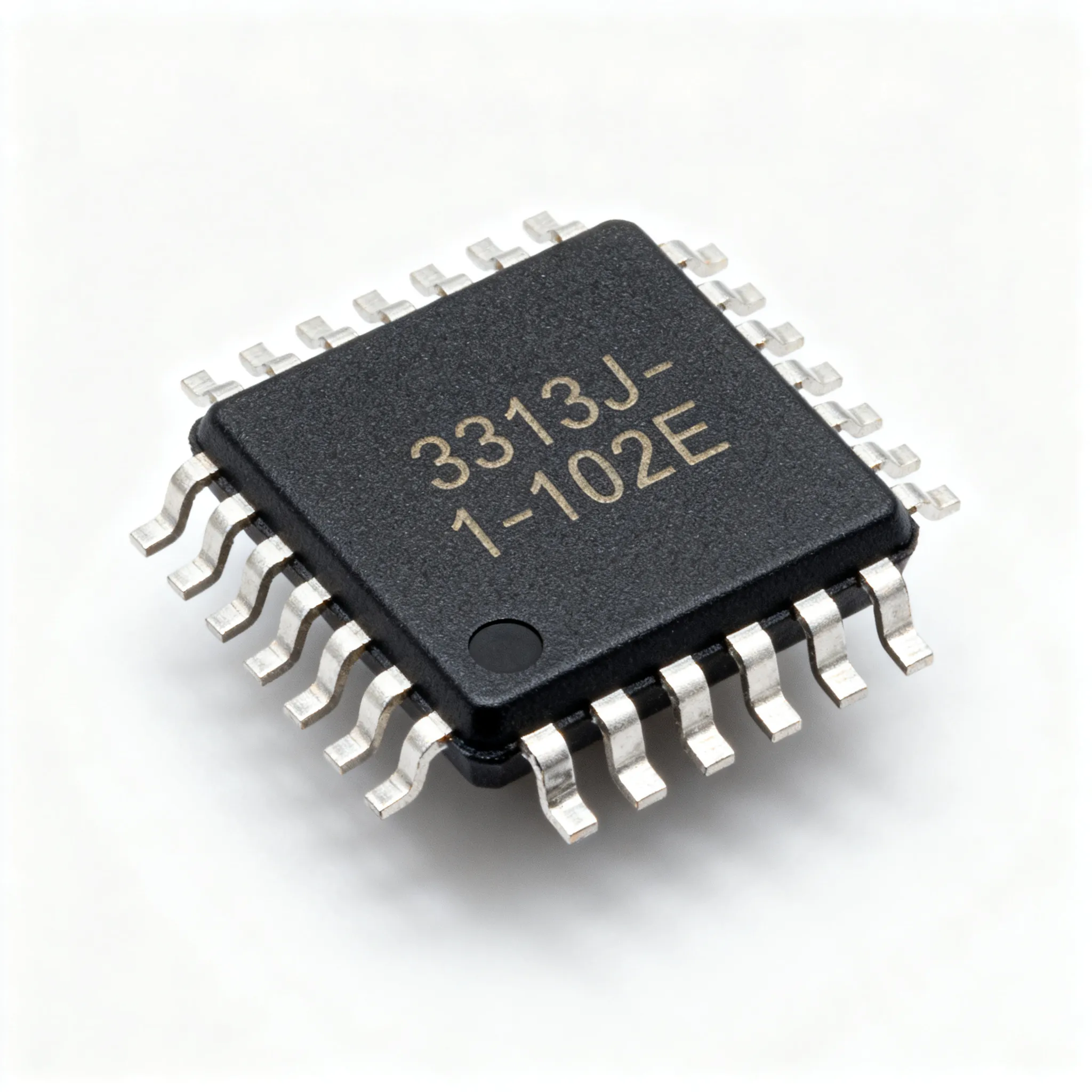
MT61K256M32JE-19G:T Datasheet and Pinout: Specs for Design and Sourcing
MT61K256M32JE-19G:T datasheet essentials, pinout overview, key specs, and design/sourcing checks for engineers and buyers. Request a quote on IC-Online.
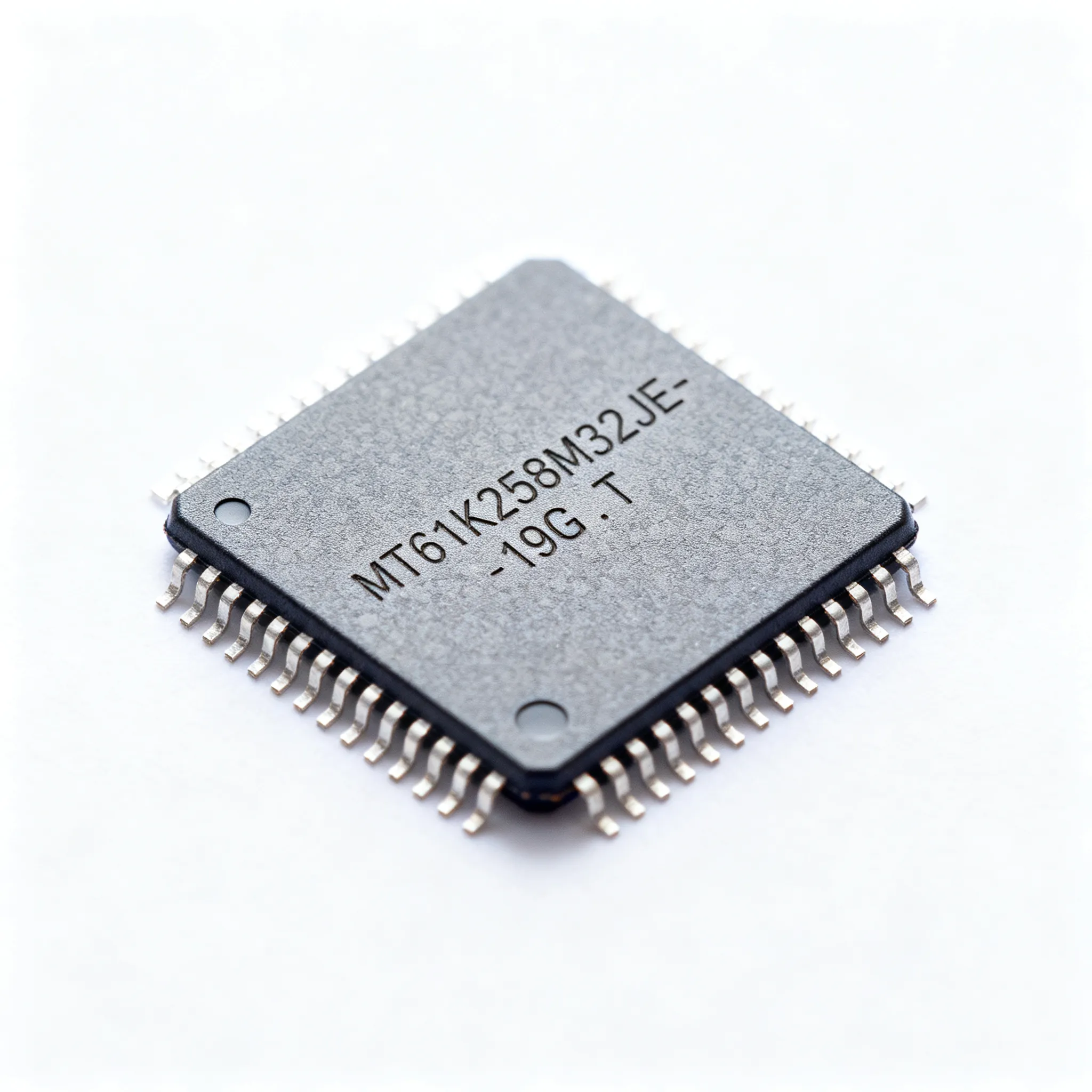
Why the MT61K256M32JE-19G:T Remains a Workhorse in GPU and Edge AI Designs
If you are designing a mid-range discrete graphics card, an edge AI inference accelerator, or a compact automotive vision module that must push tens of gigabytes per second without consuming the cost and power budget of HBM, GDDR6 remains the memory of choice. Micron’s MT61K256M32JE-19G:T sits at the sweet spot of this segment: a single 8‑Gbit, 32‑bit‑wide GDDR6 SGRAM that delivers 19 Gbps per pin while keeping PCB complexity manageable. According to recent memory market analysis on EE Times, graphics DRAM demand continues to grow on the back of AI‑driven acceleration and the long tail of GPU‑based compute, even as HBM captures the highest‑end sockets. That sustained demand puts parts like the MT61K256M32JE-19G:T squarely on the bill‑of‑materials of multiple active design cycles—and on the radar of buyers who need to secure allocation without over‑specifying.
What makes this specific Micron GDDR6 device a workhorse is not just raw bandwidth. It is the combination of a proven 180‑ball FBGA package, a mature PAM4 signaling PHY available on many SoC and GPU platforms, and a tight supply‑chain pedigree that leaves a clear paper trail when bought through authorized channels. For the engineer, the pinout demands careful signal‑integrity planning but rewards with reliable 76 GB/s per chip across a manageable 32‑bit bus. For the procurement lead, the device represents a commodity GDDR6 SKU that balances performance, cost, and long‑term availability—provided the right verification steps are taken. This article walks you through everything you must know about the MT61K256M32JE-19G:T before you commit it to a schematic or release a purchase order.
Inside the MT61K256M32JE-19G:T: Pinout, Signal Groups, and the Architecture That Delivers 19 Gbps
To integrate the MT61K256M32JE-19G:T correctly, you first need to understand how its 180 balls are mapped to logical blocks. The device organizes its 8 Gbit capacity as 256 Meg × 32, meaning each read or write transaction moves 32 bits of data across the DQ bus. A PAM4 (4‑level pulse‑amplitude modulation) scheme encodes two bits per symbol on each DQ lane, so the 19 Gbps pin data rate yields a 9.5‑Gbaud symbol rate—still fast enough that every millimeter of trace length and every decoupling capacitor matters.
The pinout groups are straightforward once you think of the chip as a synchronous, graphics‑oriented memory:
- Command/Address (CA[9:0]) lanes: Carried as differential pairs in GDDR6, typically 10 pairs, that run at a lower NRZ rate. They are used for all commands and row/column addressing.
- 32‑bit DQ bus (DQ[31:0]): The high‑speed PAM4 data lanes, broken into four byte‑lanes. Each byte‑lane includes its own Data Bus Inversion (DBI) pin and a dedicated EDC (Error Detection Code) lane for real‑time CRC coverage and per‑lane health monitoring.
- WCK and RCK clock pairs: WCK (write clock) and RCK (read clock) source‑synchronous clocks that run at half or quarter rate depending on the link training result. They are differential and demand impedance‑controlled routing with minimal intra‑pair skew.
- Miscellaneous housekeeping: Reset, ZQ calibration reference, VREFDQ, and several test/DFT pins that must be tied appropriately as per Micron’s application note.
PAM4 signaling is inherently more sensitive to amplitude noise and reflections than NRZ. The eye height shrinks; differential return loss must be kept in check. This is why Micron’s layout guide for the 180‑ball FBGA insists on tight length matching (<±1 mil within a byte‑lane for DQ signals) and low‑loss laminate. Industry guidelines such as those in IPC‑2221 help define the pad geometry and land pattern requirements for this 0.8 mm ball‑pitch BGA. Many designers also cross‑reference the IPC‑A‑610 standard when establishing acceptance criteria for BGA solder joints later in manufacturing.
Here is the quick‑reference datasheet core you will keep on your desk:
| Parameter | Value | Notes |
|---|---|---|
| Density | 8 Gbit | 256 Meg × 32 organization |
| Data rate per pin | 19 Gbps | PAM4 modulation; 9.5 Gbaud symbol rate |
| Total bandwidth per device | 76 GB/s | 32 bits × 19 Gbps / 8 |
| Supply voltage (VDD) | 1.35 V | Core supply |
| I/O voltage (VDDQ) | 1.35 V | DQ and clock I/O rail |
| Package | 180‑ball FBGA | 0.8 mm ball pitch; tray packing |
| Temperature range | 0 °C to +95 °C (TJ) | Commercial grade –G suffix |
| Signaling | PAM4 for DQ lanes; NRZ for CA | EDC and DBI supported |
| Data mask/DBI | 1 DBI pin per byte‑lane | Reduces simultaneous switching noise |
| EDC | Per‑byte‑lane CRC | Real‑time error detection; read/write EDC |
| Clock architecture | Differential WCK/RCK | Source‑synchronous; half‑rate or quarter‑rate mode |
Takeaway: The MT61K256M32JE-19G:T is not a “simple” 32‑bit SDRAM. Its architectural richness (PAM4, EDC, per‑byte DBI, and flexible clocking) is what makes it perform, but it also raises the design‑validation bar. Get the pinout right at the symbol level and you will avoid last‑minute respins caused by swapped WCK polarity or a missing VREFDQ connection.
How MT61K256M32JE-19G:T Stacks Up Against Alternative GDDR6 Parts Worth Evaluating
Your GPU or FPGA design may be able to accommodate a different GDDR6 device, but you must weigh density, speed, voltage compatibility, and the engineering effort required to swap vendors. The table below compares the MT61K256M32JE-19G:T against two neighbors in the GDDR6 landscape: Micron’s own double‑density sibling and a popular Samsung part that often appears in alternative bills‑of‑materials.
| Parameter | MT61K256M32JE-19G:T (Micron) | MT61K512M32JE-19G (Micron) | K4ZAF325BM-HC18 (Samsung) | Selection Notes |
|---|---|---|---|---|
| Density | 8 Gbit | 16 Gbit | 8 Gbit | Double density enables larger frame buffers without adding chips, but may require a different memory map. |
| Data rate | 19 Gbps | 19 Gbps | 18 Gbps | The 1 Gbps difference can impact peak throughput; account for controller support. |
| VDD / VDDQ | 1.35 V / 1.35 V | 1.35 V / 1.35 V | 1.25 V / 1.25 V | Your PMIC must supply the correct voltage; swapping from Micron to Samsung requires a regulator change or reconfiguration. |
| Package | 180‑ball FBGA | 180‑ball FBGA | 180‑ball FBGA | Same ball count, but pin map differs. A PCB re‑layout is mandatory when moving between vendors. |
| Pin compatibility | Reference (Micron J‑die) | Not pin‑compatible with 8 Gbit J‑die (different ball‑out) | Not pin‑compatible with Micron J‑die | Validate every ball in the vendor datasheet; treat devices as requiring full re‑validation. |
| Training sequences | Micron‑defined ZQ calibration and WCK‑to‑RCK training | Same Micron training flow | Samsung‑specific MRS settings and training timing | GDDR6 link training firmware is vendor‑proprietary. Switching vendors means rewriting training sequences. |
Micron’s own GDDR6 product page and Samsung’s GDDR6 SGRAM documentation both underline that while the JEDEC standard defines the broad interface class, implementation details diverge. For a buyer, that means the MT61K256M32JE-19G:T is not a casual substitute for a Samsung‑qualified socket—and vice‑versa. Evaluate any alternative as an entirely new BOM line item that demands schematic, layout, and firmware engineering time.
Design and Sourcing Rules for MT61K256M32JE-19G:T That Prevent Late-Stage Surprises
A working GDDR6 design at 19 Gbps is as much about procurement discipline as it is about SI simulation. Below are the practical rules that hardware teams and supply‑chain managers commonly enforce when the MT61K256M32JE-19G:T appears on an approved vendor list.
1. Follow Micron’s layout guide to the letter. The company publishes a detailed design guide (e.g., TN‑40‑01) that specifies trace impedance, length‑matching budgets, via backdrilling requirements, and decoupling-capacitor values. The 180‑ball FBGA demands that all DQ byte‑lanes be length‑matched within ±1 mil and that differential clocks (WCK/RCK) hit within ±0.5 mil intra‑pair. Low‑loss laminate such as Megtron 6 is recommended; ask your PCB fabricator to quote a stackup that supports a stable 40–50 Ω single‑ended and 80–100 Ω differential impedance across the required length.
2. Guard the reference clocks and power integrity. The MT61K256M32JE-19G:T uses a PLL‑based clock tree; jitter on the reference WCK path directly eats into the timing margin at the PAM4 receiver. Use a low‑jitter differential clock source and route it away from noisy switching planes. VDD and VDDQ rails must be decoupled at every ball cluster with a combination of high‑frequency 100 nF caps and bulk 10 µF ceramics. Consider dedicated power planes with sufficient copper to keep DC IR drop below 20 mV.
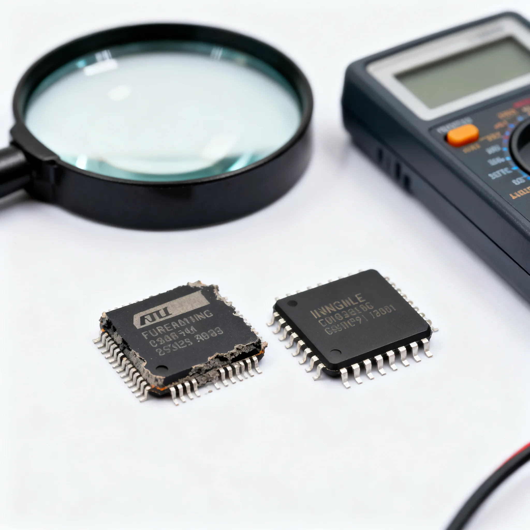
3. Never source from unauthorized resellers. GDDR6 chips are high‑value targets for remarking and re‑balling. Accept only parts that come in Micron‑branded tray packs with a traceable lot number, then visually inspect under magnification for laser‑etched markings consistent with Micron’s PCN‑verified top‑mark format. Require a certificate of conformance that references the exact manufacturer part number and DC layer. Use IPC‑A‑610 class 2 or 3 criteria to judge solder‑ball appearance, body flatness, and any evidence of re‑work.
4. Monitor lifecycle actively. The MT61K256M32JE-19G:T is a mature GDDR6 device that remains in production, but any semiconductor can transition to “last‑time buy” status with little warning. Sign up for Micron product‑change notifications and discuss lifecycle visibility with your authorized distributor on a quarterly cycle. For designs with a lifespan exceeding five years, develop a lifetime‑buy model that accounts for your annual run rate and a buffer that absorbs unplanned demand spikes.
To help engineering teams set appropriate constraints, here is a summary of the critical PCB and signal‑integrity targets you should lock early in layout:
| Design Parameter | Target | Verification Method |
|---|---|---|
| Single‑ended impedance (DQ, CA) | 40 Ω ±10% | TDR measurement on test coupon |
| Differential impedance (WCK, RCK) | 80 Ω ±10% | Differential TDR; VNA return loss up to 20 GHz |
| Intra‑lane DQ skew | < 1 mil | Layout length report; 3D EM simulation |
| Inter‑lane DQ skew (within byte‑group) | < 5 mil | Post‑route phase matching check |
| Via stub length | < 10 mil (backdrill if needed) | Cross‑section or TDR of via stub resonance |
| VDD decoupling per ball | 1 × 100 nF + 1 × 10 µF per 8 balls | PDN impedance analysis up to 100 MHz |
| Reference plane integrity | Unbroken GND below memory and controller | Visual inspection; no splits under high‑speed traces |
| Package land pad diameter | 0.35 mm NSMD | Per IPC‑2221 and Micron recommended footprint |
Following these numbers does not guarantee a first‑pass pass, but ignoring any one of them is the fastest route to a board that periodically trashes a rendering frame or fails link training at high junction temperature. Factor in at least one dedicated signal‑integrity simulation pass and a lab validation round with a known‑good Micron sample before releasing the Gerbers.
MT61K256M32JE-19G:T: What Engineers and Procurement Leads Ask
Over dozens of design review and sourcing gate meetings, certain questions about the MT61K256M32JE-19G:T come up again and again. Below are the answers that help you move from inquiry to a confident decision.
Q: What do the suffixes in MT61K256M32JE-19G:T mean?
The Micron part‑number decoder helps you confirm the exact device you are ordering. MT61K identifies the product as a GDDR6 SGRAM. 256M32 breaks down as 256 Meg × 32, giving an 8‑Gbit density. JE specifies the 180‑ball FBGA package (J‑die revision). -19 is the 19 Gbps speed grade; faster or slower bins carry different two‑digit numbers. G defines the commercial temperature range (TJ = 0 °C to +95 °C). The colon and T at the very end indicate tray packing—standard for production volumes.
Q: Can I drop this part directly into a board designed for a Samsung or Hynix GDDR6 chip?
No. While the JEDEC GDDR6 standard defines the high‑level interface and training concepts, the physical pin‑out, signal mapping, and vendor‑specific Mode Register Set (MRS) training sequences differ. A PCB originally laid out for a Samsung GDDR6 device will not accept a Micron die without a full schematic re‑map and layout respin. Your firmware must also be updated to execute the Micron‑defined ZQ calibration, WCK‑to‑RCK training, and EDC initialization. Treat cross‑vendor alternatives as new designs that require board‑level and software re‑validation from scratch.
Q: What PCB impedance and stackup should I target for reliable 19 Gbps operation?
Target 40–50 Ω single‑ended for data and command/address lanes, and 80–100 Ω differential for the WCK/RCK clock pairs. Use a low‑loss laminate such as Megtron 6 or a comparable material with a dissipation factor below 0.005 at 10 GHz. Keep intra‑lane DQ skew under 1 mil and route the differential clocks on or near the top layer with minimal vias; if vias are unavoidable, backdrill them to eliminate stubs. Decouple the VDD and VDDQ rails aggressively and consult Micron’s TN‑40‑01 layout guide for exact ball‑to‑via fanout patterns. Pre‑layout 3D EM simulation is strongly recommended.
Q: How do I confirm I'm buying genuine MT61K256M32JE-19G:T and not gray‑market parts?
Purchase exclusively through Micron’s authorized distribution network; global partners include Arrow Electronics and Avnet. When the shipment arrives, request a certificate of conformance that ties the lot number to the manufacturer’s internal trace data. Inspect the laser‑etched top mark under a microscope: the Micron logo, part number, date code, and country of origin must be crisp and consistent with the factory format. Any evidence of re‑balling, inconsistent ball‑size, or black‑topped surface indications should trigger a rejection. Reference IPC‑A‑610 class 3 visual inspection criteria when setting your incoming inspection checklist; some labs also perform X‑ray and decapsulation for high‑risk lots.
Q: Is this part suitable for automotive or extended‑temperature designs?
The commercial‑grade MT61K256M32JE-19G:T (‑G suffix) is rated for TJ 0 °C to +95 °C, which covers typical graphics cards, industrial edge systems, and indoor compute equipment but falls short of the ‑40 °C to +105 °C range demanded by most automotive ECU environments. For automotive applications, select Micron’s AEC‑Q100‑qualified GDDR6 variants, identified by an -AAT temperature suffix, and validate with your distributor that the selected speed grade and density are available under automotive grade.
Q: What is the lifecycle status of the MT61K256M32JE-19G:T and should I plan for EOL?
It is an actively produced node at Micron, but like all graphics DRAM products it is subject to end‑of‑life transition as process technologies evolve. No public EOL notice exists at the time of writing; confirm current lifecycle status by requesting a product‑change notification subscription from your distributor and checking Micron’s PCN page. For designs with a locked‑in lifetime of seven years or more, work with your authorized source to define a lifetime‑buy quantity that aligns with your production forecast. Tray‑packed inventory is easier to manage than re‑reeled, but all units should be stored in humidity‑controlled storage in accordance with J‑STD‑033.
References & Further Reading
- EE Times — Electronics Engineering News
- IPC Standards (IPC‑2221, IPC‑A‑610, J‑STD‑033)
Confirm allocation-backed availability via RFQ or BOM upload on IC-Online.