RS8452XK Design and Selection Guide for Precision Analog Circuits
Expert guide on RS8452XK Design and Selection Guide for Precision Analog Circuits. Technical specs, applications, sourcing tips for engineers and buyers.
RS8452XK Precision Amplifier Design and Selection Guide: From Specs to Supply Chain
When Instrument Clusters Go Blank: Why Precision Op Amp Selection Matters Now
A recent recall of more than 65,000 Ram trucks for blank instrument cluster displays (MoparInsiders, TFLtruck) is a sobering reminder that even a single point of failure in the analog signal chain can cascade into a safety-critical field event. The root cause in that case was a software error, but the blank screen itself represents a total loss of the driver’s visual interface—a failure mode that any precision analog front-end must be designed to withstand. For engineers specifying operational amplifiers for instrumentation, medical monitors, or battery-powered data loggers, the lesson is clear: the choice of op amp ripples through the entire signal path, and unreliable performance at the front end can mimic a software fault in the field.
Analog Devices’ reliability prediction techniques (Know Your Safety Application Notes, Part 1) highlight three industry-standard methods for estimating IC failure rates. When you apply those techniques to a precision amplifier like the RS8452XK, you see that parameters such as input bias current drift and offset voltage stability are directly tied to long-term field reliability. A part that drifts out of specification over temperature or time can cause the exact kind of silent, intermittent failure that is notoriously hard to debug—and just as expensive as a full recall. The RS8452XK addresses this by offering a 1 pA typical input bias current and a wide supply range, making it a strong candidate for high-impedance sensor front-ends where every femtoamp matters.
In the sections that follow, we’ll walk through the architecture and key specifications of the RS8452XK, compare it against a more integrated analog front-end, and provide both design and sourcing guidance that helps you avoid the pitfalls that can turn a precision amplifier into a field-return statistic.
Inside the RS8452XK: Architecture, Key Specifications, and Silent Failure Modes
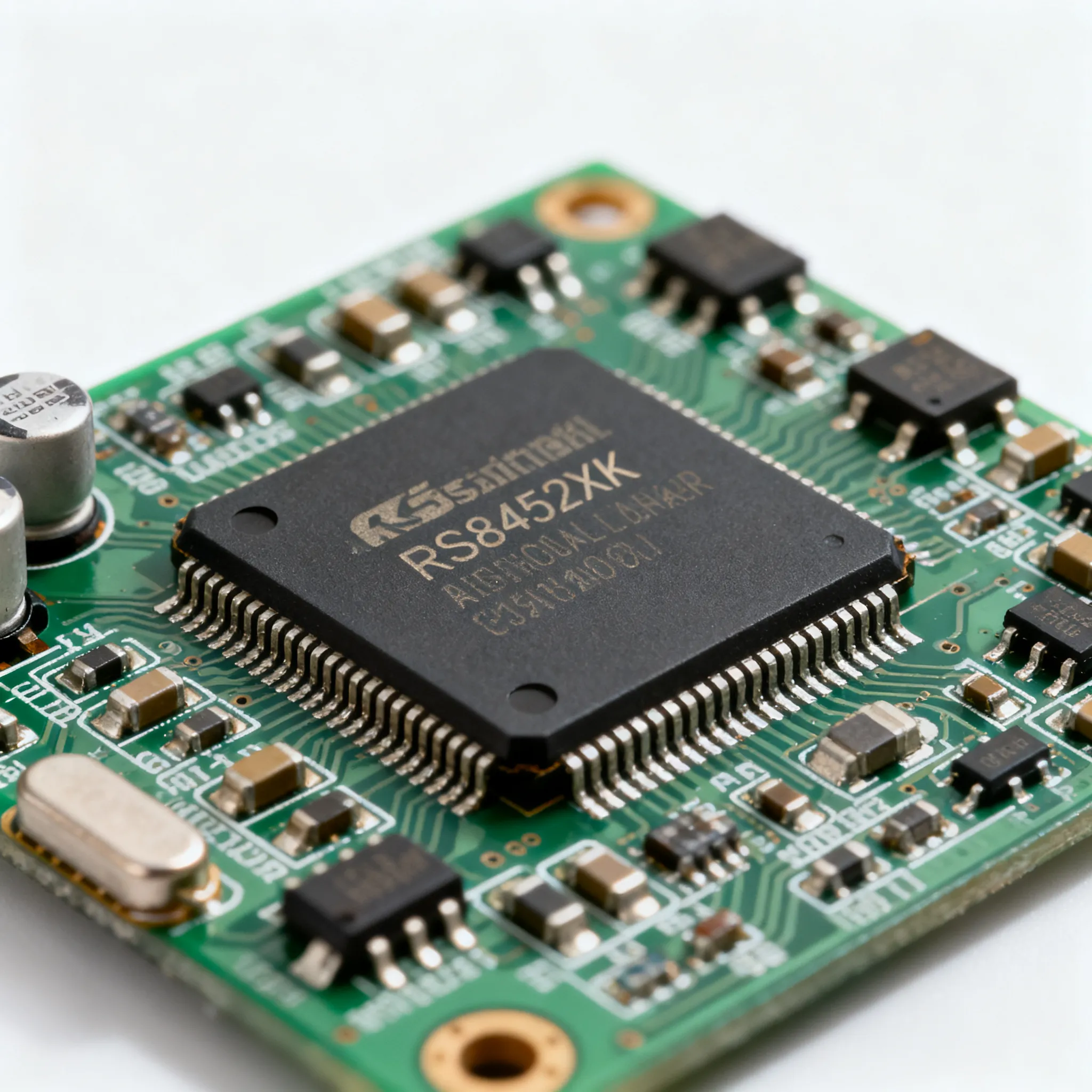
The RS8452XK is a CMOS dual operational amplifier fabricated by Runic Technology, housed in an industry-standard 8‑SOIC package (Ovaga). Each channel provides rail‑to‑rail input and output swing, a feature that becomes critical in low‑voltage battery‑powered instruments where every millivolt of headroom counts. At its heart, the amplifier uses a complementary differential input stage that achieves a typical input bias current of just 1 pA (JAK Electronics). This sub‑picoamp leakage is not a marketing number; it’s the parameter that determines whether a photodiode transimpedance amplifier will resolve a 10 nA full‑scale current or drown in its own offset error.
However, precision op amps can fail silently long before a catastrophic short. Offset voltage drift, popcorn noise, and input bias current shift over temperature are the invisible killers of measurement accuracy. Analog Devices’ precision technology signal chain strategies (Precision Technology Selection Guide) categorize these failure modes and stress that the error budget must include the worst‑case specification over the intended operating temperature range, not just the typical value at 25°C. The table below pulls the key parameters of the RS8452XK and maps them against the demands of typical precision applications.
| Parameter | RS8452XK Value | Unit / Notes |
|---|---|---|
| Supply Voltage Range | 1.8 – 5.5 | V; single‑supply operation possible |
| Input Bias Current (typical) | 1 | pA; enables direct high‑impedance sensor interfacing |
| Input Offset Voltage (max) | 5 | mV; check post‑assembly calibration if needed |
| Gain‑Bandwidth Product | 1 | MHz; sufficient for many sensor bandwidths |
| Slew Rate | 0.6 | V/µs; adequate for DC‑near‑DC precision paths |
| 0.1 Hz to 10 Hz Noise | 4 | µVpp (typical); low‑frequency noise dominates in precision DC |
| Rail‑to‑Rail I/O | Yes | Maximizes dynamic range at low supply voltages |
| Package | 8‑SOIC | Standard footprint; easy prototyping and second‑source |
What the table does not show is how these parameters interact. For example, the 1 pA input bias current assumes a clean PCB layout and a junction temperature close to ambient. Any moisture or contamination on the board can increase leakage by orders of magnitude, and thermal gradients across the input pair will dominate the offset drift. That’s why the next topic—layout—is inseparable from the datasheet specifications. Before we get there, however, it’s worth comparing the RS8452XK against a more integrated alternative to understand when a simple dual op amp wins over a full analog front-end.
RS8452XK vs. AD8452: When to Choose a Discrete Op Amp Over an Integrated AFE
The AD8452 from Analog Devices (AD8452 datasheet) is a precision analog front-end that combines a programmable gain amplifier (PGA), an ADC driver, and a precision controller all on one die. It is purpose‑built for battery test and formation systems where the signal chain must measure voltage and current with extreme accuracy over a wide dynamic range. The RS8452XK, on the other hand, is a general‑purpose dual CMOS op amp that gives you the raw building blocks. The decision between them is not about which is “better” but about which fits your system architecture and cost structure.
To help you make that choice, the comparison table below lines up the critical specifications and integration features. Following the table, we’ll discuss how the selection of an op amp flows into the rest of the signal chain, a topic that Analog Devices’ precision DAC selector guide (Precision DAC Selector Guide) illustrates for converter‑heavy designs.
| Comparison Metric | RS8452XK (Runic) | AD8452 (Analog Devices) | Selection Criteria & Failure Boundary |
|---|---|---|---|
| Input Bias Current | 1 pA typ. | 50 pA max. | For photodiodes, piezo sensors, or high‑impedance bridges, the lower bias current of the RS8452XK reduces error voltage without additional guarding. |
| Offset Voltage | 5 mV max. | ±0.5 mV max. (after autozero) | The AD8452’s integrated autozero gives lower offset, but the RS8452XK can be calibrated externally if the system uC has a calibration routine. |
| Gain‑Bandwidth Product | 1 MHz | 10 MHz (PGA bandwidth) | Higher bandwidth in the AD8452 supports fast multiplexed measurements; the RS8452XK is sufficient for DC‑to‑low‑kilohertz sensor loops. |
| Supply Voltage | 1.8 – 5.5 V | ±5 V to ±15 V (dual‑supply) | The RS8452XK’s wide single‑supply range is ideal for battery‑operated instruments; the AD8452 requires symmetric supplies, complicating portable design. |
| Integrated Features | Dual op amp only | PGA, ADC driver, precision controller | When the system already contains a dedicated ADC and MCU, the RS8452XK avoids redundant functions and reduces BOM cost. |
| Typical Cost (relative) | Lower per channel | Higher, but integrates multiple functions | For high‑volume instruments where PCB area is not the primary constraint, the discrete RS8452XK can lower the total amplifier cost. |
The AD8452’s integrated PGA and ADC driver can dramatically simplify the layout of a battery test system, but that integration locks you into a specific gain‑range and ADC input architecture. If your design uses a stand‑alone, high‑resolution ADC with its own driver, or if you need to place a buffer right at the sensor connector, the RS8452XK gives you the flexibility to optimize each stage independently. The precision DAC selector guide from Analog Devices reinforces this point: the amplifier you choose today determines the effective resolution and noise floor of the entire digitization chain, so you must evaluate the complete signal path, not just the op amp datasheet.
Both parts are available through distribution. Product pages at Ovaga Technologies and ICS-Embedded list the RS8452XK, and we recommend checking the latest inventory and lead‑time status through those channels. Before committing to a design, however, there are several layout and sourcing steps that will protect the performance you see on the datasheet.
Designing for Precision: RS8452XK Layout, EMI Hardening, and Reliable Sourcing
A 1 pA input bias current is only achievable in the real world if the PCB layout treats every high‑impedance node as a potential leakage path. Moisture, flux residue, and even the surface resistance of the solder mask can degrade the apparent bias current by nanoamps. The following table distills the layout practices that field‑proven precision designs use to preserve the native performance of the RS8452XK.
| Design Practice | Purpose | Failure Mode Avoided |
|---|---|---|
| Guard rings around the inverting input | Divert leakage current from nearby traces to a low‑impedance node | Leakage‑induced offset voltage that mimics a sensor error |
| Short, direct traces from sensor to op amp input | Minimize parasitic capacitance and antenna area | Noise coupling and phase shift in feedback loop |
| 10 µF tantalum + 0.1 µF ceramic decoupling at each supply pin | Suppress low‑frequency and high‑frequency supply ripple | Oscillation and power‑supply‑induced offset drift |
| Thermal symmetry in the input pair layout | Keep both input transistors at the same temperature | Thermocouple‑induced offset drift (Seebeck effect) |
| Keep the amplifier away from high dV/dt nodes (switching regulators, digital buses) | Reduce capacitive coupling of fast edges | EMI‑induced DC offset shift |
After the layout is optimized, the sourcing plan must be equally rigorous. The Ram instrument cluster recall (MoparInsiders) shows that even a non‑safety‑critical display failure can trigger a large‑scale field action. While the RS8452XK is not specifically AEC‑Q100 qualified, it can still be used in non‑safety‑critical automotive display circuits if you perform additional qualification. The failure rate analysis techniques from Analog Devices’ application notes (Know Your Safety Part 1) give you a framework to estimate the reliability of the amplifier in your specific operating profile. Engineering teams should insist on getting the worst‑case specification limits over the full temperature range, not just the typical values, and should build a second‑source strategy around parts that match the critical 1 pA bias current and rail‑to‑rail I/O capability.
For immediate procurement, we recommend verifying current lead times and stock through the distributor links provided earlier. Building a resilient supply chain for precision amplifiers also means looking at the entire signal chain. The Analog Devices precision DAC selector guide (Precision DAC Selector Guide) can help you identify alternative DAC‑driver combinations that are pin‑compatible with your design, reducing the risk of a single‑source bottleneck.
Your RS8452XK Questions, Answered by Precision Analog Engineers
Q: What is the typical input bias current of the RS8452XK and how does it affect high‑impedance sensor circuits?
The RS8452XK has a typical input bias current of 1 pA (JAK Electronics). This extremely low current allows direct interfacing with high‑impedance sensors such as photodiodes and piezoelectric transducers without significant voltage error, eliminating the need for additional buffer stages.
Q: Can the RS8452XK operate from a single 3.3 V supply for battery‑powered instruments?
Yes. The RS8452XK’s supply voltage range of 1.8 V to 5.5 V (Ovaga) supports single 3.3 V operation, making it ideal for battery‑powered data loggers and portable medical devices. Rail‑to‑rail inputs and outputs maximize dynamic range even at low supply voltages.
Q: How does the RS8452XK compare to the AD8452 for precision ADC driving?
The AD8452 (datasheet) integrates a programmable gain amplifier and ADC driver, offering higher integration for battery test and precision measurement systems. The RS8452XK is a discrete dual op amp with ultra‑low bias current, giving designers more flexibility and lower cost in simple buffering, filtering, or gain stages where the AD8452’s extra features are not needed.
Q: What PCB layout techniques are critical to maintain low offset drift?
Guard rings around the high‑impedance inputs, short traces, and a clean supply with proper decoupling (10 µF tantalum in parallel with 0.1 µF ceramic) are essential. Keep the amplifier away from high dV/dt nodes and use thermal symmetry to minimize thermocouple effects, referencing the layout practices in Analog Devices’ precision technology selection guide (Precision Technology Selection Guide).
Q: Is the RS8452XK suitable for automotive instrument clusters?
The RS8452XK is not specifically AEC‑Q100 qualified. However, it can be used in non‑safety‑critical automotive display circuits if the design team performs additional qualification. The recent Ram instrument cluster recall (MoparInsiders) demonstrates the high cost of signal‑chain failures and underscores the need for thorough testing and reliability analysis, as outlined in Analog Devices’ failure rate application notes (Know Your Safety Part 1).
Q: Where can I find reliable stock and avoid lead‑time risks for the RS8452XK?
Authorized distributors like Ovaga Technologies and ICS-Embedded currently list the RS8452XK. For long‑term supply resilience, cross‑reference availability with the Analog Devices precision DAC selector guide (Precision DAC Selector Guide) to identify alternative signal‑chain components and maintain a second‑source strategy.
References & Further Reading
- Ram Recalls 65,348 Trucks Over Instrument Cluster Failure – MoparInsiders
- Ram Recalls 72,000 Trucks for Blank Instrument Cluster Displays – TFLtruck
- Know Your Safety Application Notes—Part 1: Failure Rates – Analog Devices
- RS8452XK Product Page – Ovaga Technologies
- RS8452XK Specifications – JAK Electronics
- Precision Technology Selection Guide – Analog Devices
- AD8452 Datasheet – Analog Devices
- RS8452XK Listing – ICS-Embedded
- Precision DAC Selector Guide – Analog Devices
Whether you are finalizing a precision analog front‑end or need to secure a stable supply of the RS8452XK for your next production run, IC‑Online can help you navigate the component landscape. Request a quote or upload your BOM to explore mixed‑BOM support and flexible MOQ options tailored to your project.