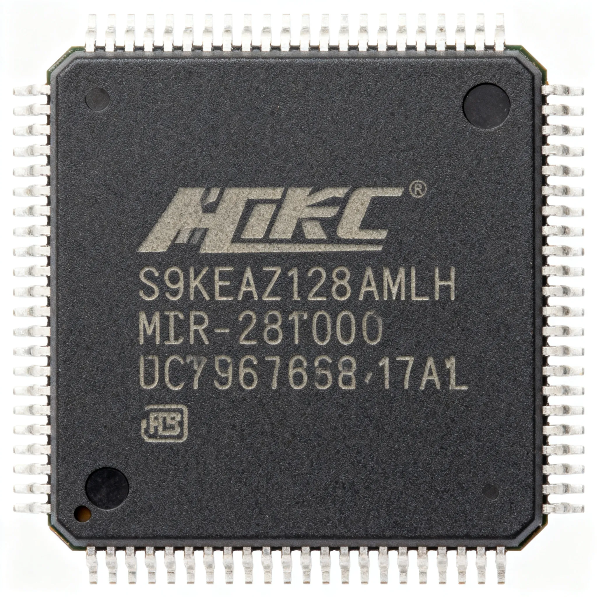
S9KEAZ128AMLH Datasheet and Pinout: Specs for Design and Sourcing
S9KEAZ128AMLH datasheet essentials, pinout overview, key specs, and design/sourcing checks for engineers and buyers. Request a quote on IC-Online.
Why the S9KEAZ128AMLH Remains a Staple in Automotive and Industrial Embedded Design
The S9KEAZ128AMLH, a member of NXP's KEA family built around the Arm Cortex-M0+ core, occupies a rare sweet spot in embedded design. It delivers 5‑V tolerant I/O, integrated CAN and LIN controllers, and a −40°C to +125°C operating range — all in a compact 64‑LQFP package — making it a natural fit for body electronics, smart actuators, and industrial sensor nodes that must survive harsh electrical and thermal environments. Industry analysis from EE Times confirms that demand for automotive-grade microcontrollers with robust mixed‑signal capability has remained resilient, driven by the steady expansion of zonal architectures and electrification sub‑systems where legacy 5‑V sensor interfaces still dominate.
For procurement buyers, the S9KEAZ128AMLH represents a mature, well‑documented part backed by NXP's product longevity program. Rather than chasing the newest process node, many design teams deliberately anchor their BOMs on this device because its pinout, peripheral set, and toolchain ecosystem are proven across multiple vehicle platforms and industrial automation lines. The 128 KB on‑chip flash and 16 KB SRAM provide enough headroom to run a real‑time operating system, manage CAN/LIN communication stacks, and execute modest signal‑processing routines without forcing an external memory bus — a combination that keeps PCB area and BOM cost in check. When you couple that with a single‑supply 2.7–5.5 V operating range, the S9KEAZ128AMLH eliminates the level‑translation headaches that plague low‑voltage‑only MCUs in mixed‑voltage systems.
Still, treating this part as a commodity is a mistake. Subtle differences in analog front‑end performance, flash endurance, and supply sequencing separate the KEA family from superficially similar Cortex‑M0+ competitors. The sections that follow unpack the datasheet essentials, map the 64‑LQFP pinout, compare the S9KEAZ128AMLH against adjacent variants and external alternatives, and offer practical design‑and‑sourcing guidance that helps both engineers and buyers move from schematic capture to production with confidence. Throughout, the emphasis is on verifiable, datasheet‑grounded information — not market speculation or unqualified drop‑in claims.
Decoding the S9KEAZ128AMLH Datasheet: Core Architecture, Memory Map, and Pinout Essentials
A disciplined reading of the S9KEAZ128AMLH datasheet — available directly from NXP's product page — reveals a microcontroller that balances processing throughput with peripheral density. At its heart sits a 48 MHz Arm Cortex-M0+ core implementing the ARMv6‑M architecture, which delivers approximately 0.93 DMIPS/MHz while consuming under 60 µA/MHz in active run mode. The core connects to a single‑cycle I/O port interface and a lightweight AHB‑Lite bus matrix, ensuring deterministic access to the 128 KB on‑chip flash (with up to 100,000 erase/program cycles per block) and 16 KB of SRAM. A 256‑byte flash‑based EEPROM emulation region spares you from adding an external non‑volatile memory IC for calibration constants or serial‑number storage.
| Parameter | Value / Range | Unit / Notes |
|---|---|---|
| CPU Core | Arm Cortex‑M0+ (ARMv6‑M) | 48 MHz maximum frequency |
| On‑Chip Flash | 128 | KB; 100k erase/program cycles (typ.) |
| On‑Chip SRAM | 16 | KB; single‑cycle access via AHB‑Lite |
| EEPROM Emulation | 256 | Bytes (flash‑backed); wear‑leveled in firmware |
| Operating Voltage | 2.7 – 5.5 | V; single‑supply, on‑chip voltage regulator |
| Ambient Temperature Range | −40 to +125 | °C; automotive Grade‑1 qualified |
| I/O Pin Count | Up to 57 | GPIO (64‑LQFP); 5‑V tolerant on most pins |
| ADC | 16‑channel, 12‑bit SAR | Up to 1 Msps; internal bandgap reference |
| Analog Comparator | 2 × ACMP | Rail‑to‑rail inputs; 5‑V operation |
| Timers / PWM | FTM (6‑ch), PIT (2‑ch), SysTick, RTC | Complementary PWM with dead‑time insertion |
| Communication Interfaces | 2 × SCI (UART), 2 × SPI, 1 × I²C, 1 × CAN 2.0B, 1 × LIN | CAN supports up to 1 Mbit/s; LIN 2.1 compliant |
| Debug / Trace | SWD (2‑wire) | Single‑wire debug plus clock; no ETM trace |
| Package | 64‑LQFP (10 × 10 mm, 0.5 mm pitch) | Exposed pad variant; MSL‑3 moisture sensitivity |
The pinout of the S9KEAZ128AMLH in the 64‑LQFP package is organized into logical port groups — PORTA through PORTE — with each pin supporting up to four alternate functions selected through the PORTx_PCRn registers. Power routing is straightforward: VDD and VSS pairs are distributed symmetrically across the package edges to minimize supply‑loop inductance. Pin 1 (PTA0) serves dual duty as the SWD_CLK debug clock, while pin 2 (PTA1) functions as SWD_DIO — meaning your debug header can be as minimal as a 4‑pin 0.05‑inch header (VDD, SWD_CLK, SWD_DIO, GND). The external crystal oscillator connects across pins 46 and 47 (EXTAL/XTAL), supporting 4–20 MHz fundamental‑mode crystals with an on‑chip Pierce oscillator. For CAN‑based designs, the CAN_TX and CAN_RX signals appear on PTC6 and PTC7 respectively, simplifying the layout by co‑locating the CAN transceiver interface on one port bank.
Tip: When laying out the 64‑LQFP footprint, treat the exposed die‑attach pad (pin 65) as a mandatory thermal and electrical ground connection. Floating the pad compromises both EMC performance and thermal dissipation. A 3×3 array of 0.3 mm thermal vias to the internal ground plane is a proven starting point for Class‑2 and Class‑3 designs, consistent with IPC‑A‑610 workmanship standards.
The clock distribution tree deserves particular attention. From the 48 MHz core clock, the bus clock (BUSCLK) can be divided down to conserve power, while the flash clock (FLASHCLK) typically runs at 24 MHz to stay within the flash access‑time window. The internal 1 kHz low‑power oscillator (LPO) keeps the RTC ticking in stop and standby modes, drawing less than 1 µA. If your application demands external clock precision for CAN bit‑timing compliance, a 4, 8, or 16 MHz crystal with ±100 ppm frequency tolerance across the full temperature range is recommended — the CAN protocol's bit‑timing constraints are unforgiving with low‑cost ceramic resonators.
S9KEAZ128AMLH Versus Alternatives: Evaluating KEA Family Variants and Competitive MCUs
The S9KEAZ128AMLH does not exist in isolation. NXP's KEA family spans multiple flash densities and package configurations, and competing silicon from other vendors targets the same 5‑V‑tolerant, CAN‑equipped Cortex‑M0+ slot. Making an informed selection requires understanding what changes — and what stays the same — when you step up, down, or across the product landscape.
| Comparison Metric | S9KEAZ128AMLH (NXP KEA128) | S9KEAZ64AMLH (NXP KEA64) | S9KEAZ128AVLH (NXP KEA128, 80‑LQFP) | STM32G0B1VCT6 (STMicro, Cortex‑M0+) | Selection Criteria & Failure Boundary |
|---|---|---|---|---|---|
| Flash / SRAM | 128 KB / 16 KB | 64 KB / 8 KB | 128 KB / 16 KB | 256 KB / 144 KB | Flash ≥ 2× code size plus OTA buffer; SRAM must cover stack + heap + RTOS overhead |
| Package | 64‑LQFP (10×10 mm) | 64‑LQFP (pin‑compatible) | 80‑LQFP (12×12 mm) | 64‑LQFP (10×10 mm) | Footprint identical for 64‑LQFP; 80‑LQFP gains 16 extra I/O |
| Supply Voltage | 2.7–5.5 V | 2.7–5.5 V | 2.7–5.5 V | 1.7–3.6 V | 5‑V systems must use KEA; 3.3‑V designs can evaluate STM32G0 |
| 5‑V Tolerant I/O | Yes (most pins) | Yes | Yes | No (3.6 V max) | Legacy sensor/actuator interfaces demand true 5‑V tolerance |
| CAN / LIN | 1 × CAN 2.0B + 1 × LIN 2.1 | 1 × CAN + 1 × LIN | 1 × CAN + 1 × LIN | 2 × FDCAN + 1 × USART/LIN | CAN‑FD future‑proofs; KEA suits classic CAN/LIN body networks |
| ADC Resolution / Rate | 12‑bit / 1 Msps | 12‑bit / 1 Msps | 12‑bit / 1 Msps | 12‑bit / 2.5 Msps | Higher sample rate benefits motor‑control current loops |
| DMA Channels | None (CPU‑only) | None | None | 12‑channel DMA + DMAMUX | DMA offloads CPU; critical for high‑throughput sensor streams |
| Reference Hardware / SDK | FRDM‑KEA128 + MCUXpresso SDK | FRDM‑KEA64 | Custom 80‑LQFP eval board | NUCLEO‑G0B1RE + STM32CubeG0 | Availability of low‑cost eval boards accelerates prototyping |
| Product Longevity Program | NXP 15‑year (KEA family) | Same | Same | STM32 10‑year (G0 series) | Verify current status with manufacturer before BOM lock |
Within the KEA family, the S9KEAZ128AMLH and the S9KEAZ64AMLH share an identical 64‑LQFP pinout and peripheral mapping — a deliberate design choice that lets teams develop on the 128 KB part and cost‑reduce to 64 KB once firmware size is proven. However, the SRAM halves from 16 KB to 8 KB, which can be a trap if your application dynamically allocates large buffers or uses a RAM‑intensive RTOS tick. The S9KEAZ128AVLH, with its 80‑LQFP package, exposes an additional 16 I/O pins — useful when you need extra GPIO or a second SPI instance — but the larger 12×12 mm footprint may push your board outline past a tight enclosure constraint.
Stepping across to STMicro's STM32G0B1VCT6 reveals a fundamentally different design philosophy. The STM32G0 offers substantially more SRAM (144 KB), a 12‑channel DMA controller, and CAN‑FD support — features that excel in data‑intensive sensor‑fusion nodes or gateways that aggregate multiple CAN buses. But the STM32G0's I/O is not 5‑V tolerant, which means every legacy 5‑V sensor signal must pass through a level translator or resistive divider. In a 24‑V vehicle or industrial bus architecture where sensor power rails routinely sit at 5 V, that single difference can add $0.30–$0.80 in BOM cost and 10–15 mm² of PCB area per channel. Furthermore, any alternative — whether a KEA family variant or an external competitor — must be re‑qualified against your system's EMC, brown‑out, and watchdog‑timeout behavior. Subtle differences in analog channel crosstalk, power‑on reset threshold, or flash‑write current profile can manifest as intermittent field failures that only surface after hundreds of temperature cycles.
Key Takeaway: The S9KEAZ128AMLH is the 5‑V, classic‑CAN baseline. Evaluate KEA64 for cost‑optimized variants, KEA128‑80LQFP for extra I/O, and STM32G0 for CAN‑FD/DMA‑intensive designs at 3.3 V — always verifying pinout, firmware, and qualification before committing to an alternative.
Design and Sourcing Tips for the S9KEAZ128AMLH: From Schematic to Production Readiness
Getting the most from the S9KEAZ128AMLH demands attention to both hardware engineering fundamentals and procurement discipline. The following practices, distilled from years of field experience, help avoid the most common pitfalls that delay production schedules or inflate warranty returns.
Hardware Design Essentials:
- Crystal placement and guard ring: Position the 4–16 MHz crystal within 10 mm of the EXTAL/XTAL pins (pins 46/47). Surround the oscillator circuit with a continuous ground guard ring on all PCB layers, stitched with vias every 2–3 mm. Avoid routing any high‑speed digital trace — especially CAN_TX or PWM outputs — parallel to the oscillator traces.
- Decoupling capacitor layout: Place a 100 nF X7R ceramic capacitor within 3 mm of each VDD/VSS pin pair, with the smallest possible loop area. Add a single 10 µF bulk capacitor near the package center. The 5‑V tolerant I/O structure has relatively high dI/dt during simultaneous pin switching; inadequate decoupling manifests as ADC noise floors that climb by 2–3 LSBs under worst‑case I/O toggling.
- SWD debug header accessibility: Bring out SWD_CLK, SWD_DIO, VDD, and GND to a 4‑pin 0.05‑inch header even on production boards. A 100‑mil‑pitch adapter cable costs a few dollars but saves hours when in‑field firmware updates or failure analysis is required. Include a 10 kΩ pull‑up on SWD_DIO and a 10 kΩ pull‑down on SWD_CLK to ensure the debug interface remains stable during power‑cycling.
- CAN bus termination and filtering: The integrated CAN controller requires an external transceiver (e.g., TJA1050 or MCP2551). Place the transceiver's VCC decoupling capacitor close to its supply pin, and route the CAN_H/CAN_L traces as a tightly coupled differential pair with 120 Ω characteristic impedance. A split‑termination network (two 60 Ω resistors with a 4.7 nF capacitor to ground at the center tap) improves common‑mode noise rejection in electrically noisy engine‑compartment or motor‑drive environments.
- Unused pin termination: Configure unused I/O pins as outputs driven low, or as inputs with internal pull‑ups enabled, through the PORTx_PCRn registers during initialization. Floating inputs invite noise‑induced shoot‑through current in the pad input buffers — a phenomenon that can add 2–5 mA of unnecessary supply current in a quiet system.
- Analog input conditioning: The 12‑bit ADC's input impedance is approximately 5 kΩ at 1 Msps. For sensors with output impedance above 500 Ω, insert an external rail‑to‑rail op‑amp buffer to avoid gain errors from resistive divider loading. Maintain the ADC sampling time at a minimum of 2 µs when the analog source impedance exceeds 1 kΩ to allow the internal sample‑and‑hold capacitor to settle within ½ LSB.
Sourcing and Procurement Best Practices:
On the procurement side, the S9KEAZ128AMLH is manufactured by NXP and distributed through a network of franchised partners. Buyers should treat supply as allocation‑sensitive — particularly during periods of high automotive production volume — and confirm current availability through a request for quotation (RFQ) rather than relying on website stock‑status indicators, which may lag real‑time warehouse data by 24–48 hours.
| Sourcing Checkpoint | What to Require / Verify | Rationale |
|---|---|---|
| Authorized Distribution | Purchase only through NXP‑authorized franchised distributors | Guards against counterfeit, relabeled, or electrically degraded parts from unauthorized brokers |
| Date / Lot Code Traceability | Request lot‑code‑level traceability documentation with each shipment | Enables targeted containment if NXP issues a product change notification (PCN) or errata update |
| Moisture Sensitivity | Confirm MSL‑3 handling; reject packages with breached moisture‑barrier bags | 64‑LQFP with exposed pad is prone to popcorning during reflow if moisture has ingressed |
| Visual Inspection Criteria | Reference IPC‑A‑610 Class 2 or 3 for solder joint acceptance | Exposed‑pad solder voids exceeding 25% of pad area degrade thermal performance and long‑term reliability |
| Allocation‑Backed Lead Time | Obtain written lead‑time confirmation tied to a specific allocation quantity | Verbal lead‑time estimates without allocation commit do not guarantee supply; confirm via RFQ |
| Functional Testing of Secondary‑Market Parts | If non‑franchised sources are evaluated, require full electrical testing per datasheet limits at −40°C and +125°C | Logic‑level testing at room temperature does not expose marginal flash cells or degraded ESD structures |
The moisture‑sensitivity dimension is frequently overlooked by teams accustomed to smaller QFN or TSSOP packages. The 64‑LQFP exposed‑pad configuration (MSL‑3) requires floor‑life tracking per J‑STD‑020. Once the moisture‑barrier bag is opened, parts must be mounted within 168 hours in a factory environment held at ≤30°C and ≤60% relative humidity, or they must be baked at 125°C for 24 hours before reflow. Skipping this step can produce micro‑cracks in the mold compound that pass electrical test but grow into corrosion sites after months of field temperature cycling.
For assembly inspection, IPC‑A‑610 Class 2 criteria are the typical baseline for industrial electronics, while Class 3 is appropriate for automotive safety‑related systems where a field failure could affect occupant safety. The exposed pad demands particular scrutiny: X‑ray inspection is the only reliable method to quantify void percentage beneath the pad, and a void area exceeding 25% of the total pad area should trigger a process parameter review with your assembly partner.
S9KEAZ128AMLH Engineering and Procurement FAQs
Q: What development tools and IDEs support the S9KEAZ128AMLH?
NXP offers the MCUXpresso IDE and S32 Design Studio, both available at no cost, with direct SDK support for the KEA family. MCUXpresso integrates pin‑configuration, clock‑tree, and peripheral‑initialization tools that generate C code matching the S9KEAZ128AMLH register map. For teams working in safety‑critical applications, commercial toolchains such as IAR Embedded Workbench and Arm Keil MDK provide advanced optimization, MISRA‑C checking, and debug‑trace features that accelerate certification audits. All four environments support the SWD debug interface through standard debug probes like SEGGER J‑Link, P&E Multilink, and NXP's LPC‑Link2.
Q: Where can I find the exact pinout for the 64‑LQFP package?
The official pinout diagram and signal‑multiplexing table reside in the S9KEAZ128AMLH datasheet (document number S9KEAZ128AMLH) and the KEA128 Reference Manual, both downloadable from NXP's product page. The hardware design files — available as part of the FRDM‑KEA128 evaluation board package — include a pinout spreadsheet that assigns each of the 64 physical pins to its default GPIO function, analog channel, and alternate communication modules. Engineers should always cross‑reference the datasheet revision against the silicon revision stamped on the package to catch any pin‑function errata.
Q: Is the KEA family still recommended for new designs?
Yes. The KEA family is covered under NXP's product longevity program, which commits to extended supply for automotive and industrial customers. New designs targeting body electronics, HVAC controllers, seat modules, and industrial actuator drives can confidently adopt the S9KEAZ128AMLH. As with any mature microcontroller, design teams should periodically review NXP's product status page for any life‑cycle updates, PCNs, or mask‑set revisions before freezing the BOM for production.
Q: Can I directly replace an S9KEAZ128AMLH with an S9KEAZ64AMLH if I need less flash?
The S9KEAZ64AMLH and the S9KEAZ128AMLH are pin‑compatible within the 64‑LQFP package and share identical peripheral mapping, pin multiplexing, and electrical characteristics. However, the flash size halves to 64 KB and SRAM to 8 KB. Firmware must be recompiled to fit within the smaller memory map — specifically, the upper flash boundary drops from 0x0001_FFFF to 0x0000_FFFF, and any linker scripts, vector‑table offsets, or flash‑resident data tables must account for the reduced range. Code that compiles to 62 KB on the 128‑KB part simply will not fit on the 64‑KB variant without optimization or feature removal. Treat this as a re‑qualification exercise, not a trivial drop‑in.
Q: What is the typical lead time and how can I mitigate sourcing risks?
Lead times for the S9KEAZ128AMLH fluctuate with foundry allocation and global semiconductor demand cycles. Buyers should work with authorized NXP distributors to secure allocation‑backed lead‑time commitments and consider buffer‑stock agreements that smooth supply during demand spikes. If secondary‑market parts are evaluated as a stop‑gap, require full electrical testing against datasheet specifications at both −40°C and +125°C corners — room‑temperature pass/fail testing is insufficient to detect marginal flash endurance or degraded ESD protection structures. Counterfeit or relabeled parts remain a risk on the open market; lot‑code traceability and visual inspection per IPC‑A‑610 criteria provide a baseline defense.
Q: What is the input voltage tolerance and ESD rating?
Most general‑purpose I/O pins on the S9KEAZ128AMLH are 5‑V tolerant regardless of the VDD supply voltage — a design feature that allows direct connection to legacy 5‑V sensors, switches, and actuator drivers without external level‑translation ICs. Exceptions include the true open‑drain pins and the RESET pin, whose voltage limits are detailed in the datasheet's pin‑characteristics table. The device's ESD protection is specified per the Human Body Model (HBM) and Charged Device Model (CDM); typical values meet or exceed 2 kV HBM and 500 V CDM, consistent with automotive‑grade robustness expectations. For systems requiring higher ESD immunity at the connector interface, external TVS diodes on CAN, LIN, and ADC input lines remain recommended.
References & Further Reading
- NXP KEA128 Product Page — Official datasheets, reference manuals, and application notes for the KEA family.
- EE Times — Electronics engineering news and analysis covering automotive MCU trends.
- IPC Standards — IPC‑A‑610 solder‑joint acceptance criteria and J‑STD‑020 moisture‑sensitivity classification.
- MCUXpresso IDE — NXP's free integrated development environment with KEA SDK support.
- S32 Design Studio — NXP's Eclipse‑based IDE for automotive and industrial MCUs.
- IAR Embedded Workbench — Commercial IDE with MISRA‑C compliance and advanced debugging for Arm Cortex‑M targets.
- Arm Keil MDK — Professional toolchain for Cortex‑M microcontrollers with safety documentation packages.
- STM32G0B1VCT6 Product Page — STMicro 256 KB Cortex‑M0+ MCU with CAN‑FD; an alternative for 3.3‑V designs.
- IC-Online — Request a quote or upload your BOM for the S9KEAZ128AMLH and associated components.
Whether you are finalizing a schematic for a next‑generation body control module or negotiating allocation for an existing production line, the S9KEAZ128AMLH rewards a thorough understanding of its datasheet, pinout, and supply‑chain dynamics. The part's 5‑V tolerance, integrated CAN/LIN, and automotive temperature range make it a resilient choice for mixed‑signal embedded systems — but those same strengths depend on disciplined decoupling layout, proper moisture‑sensitivity handling, and sourcing through authorized channels. For current pricing, availability, and allocation‑backed lead‑time quotes, visit IC