

SGT60N60FD1P7 Datasheet and Pinout: Specs for Design and Sourcing
SGT60N60FD1P7 datasheet essentials, pinout overview, key specs, and design/sourcing checks for engineers and buyers. Request a quote on IC-Online.
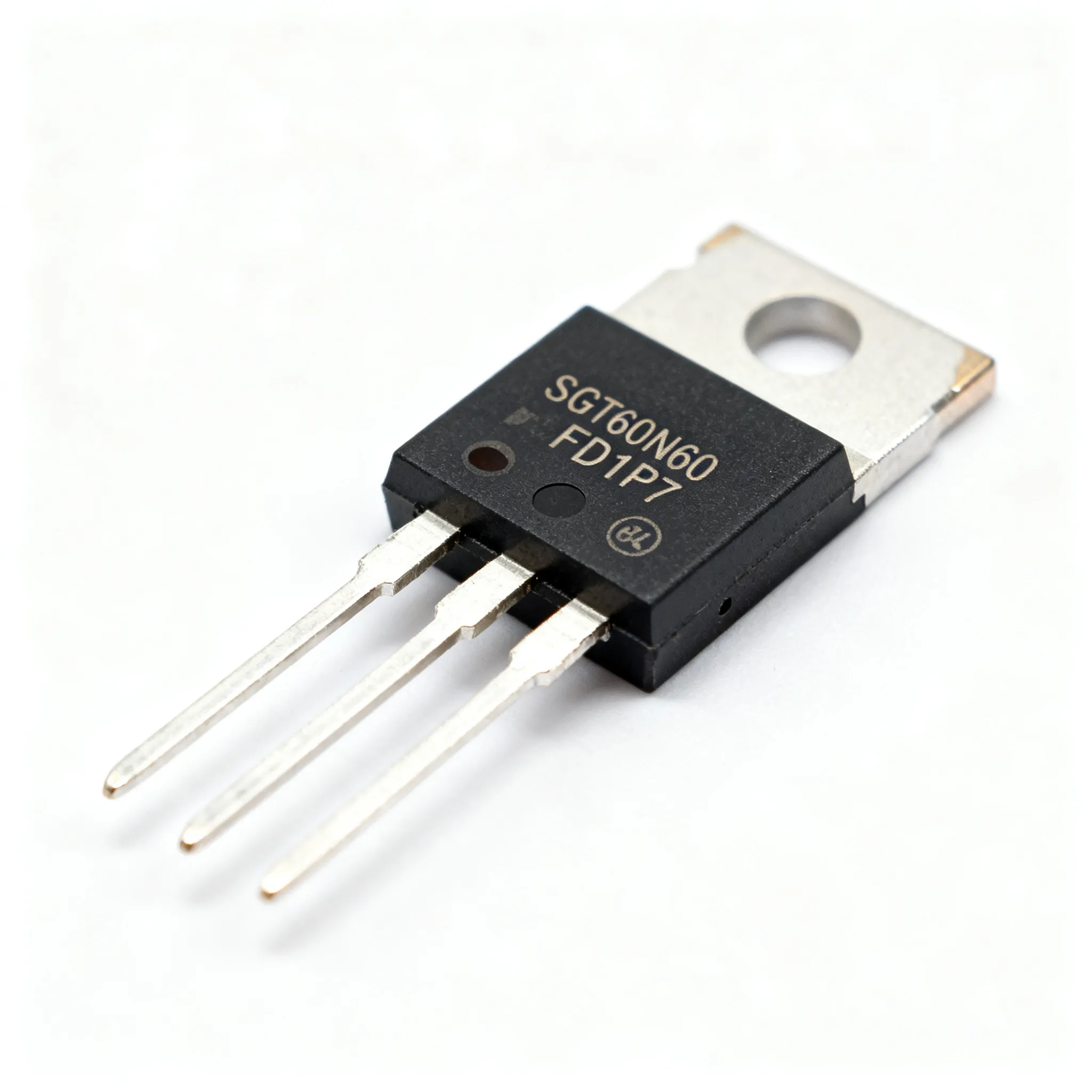
Why the SGT60N60FD1P7 Pinout Confusion Still Trips Up Design Reviews
Even in mature 600 V field‑stop IGBT families, a simple pinout mismatch can halt a design review dead in its tracks. The SGT60N60FD1P7 from Silan Microelectronics illustrates why: part‑number suffixes such as P7, PN, PS, and PT share a combined datasheet, yet their tab connections and diode‑catcher arrangements differ. Engineers who rely on aggregated cross‑reference tools that flatten Silan’s numbering into a single generic symbol are especially vulnerable. The family datasheet hosted at Silan’s partner site (SGT60N60FD1PN/P7/PS/PT) covers four variants in one document. If the reviewer only glances at the first page pin sketch, the SGT60N60FD1P7’s actual emitter‑tab arrangement can be misinterpreted—a risk that escalates when second‑source candidates are being evaluated.
In practice, verifying the SGT60N60FD1P7 pinout directly against the official Silan drawing is now a routine design‑review gate, particularly after field‑returns traced to heatsink shorts. The “FD1” suffix means a field‑stop IGBT with an integrated fast‑recovery diode, but the trailing P7 locks in a specific lead‑frame arrangement. When a team considers dropping in a sibling like the SGT60N60FD1PN because of perceived availability, the tab assignment can flip the high‑voltage bus to the heatsink. Checking the family document becomes a non‑negotiable step, not an afterthought.
Pin‑by‑Pin and Key Specs of the 600 V Field‑Stop SGT60N60FD1P7
Packaged in a standard TO‑247‑3, the SGT60N60FD1P7 follows the conventional IGBT pinout: Gate (G) on pin 1, Collector (C) on pin 2, and Emitter (E) on pin 3. The exposed metal tab is internally connected to the emitter, a detail that immediately influences isolation and heatsink design. When you bolt the device to a shared heatsink, the tab’s emitter potential demands an insulating pad and thermal grease to avoid shorting the collector‑emitter loop through the chassis.
The core electrical parameters that shape thermal and switching design are summarized below. Values are drawn from the SGT60N60FD1P7‑specific datasheet page at datasheet4u.com and cross‑checked against the Silan combined datasheet for guaranteed min/max limits.
| Parameter | Value/Range | Unit/Conditions |
|---|---|---|
| Collector‑Emitter Voltage, VCES | 600 | V, Tj = 25 °C to 175 °C |
| Continuous Collector Current, IC | 60 (Tc = 100 °C) | A |
| Pulsed Collector Current, ICM | 120 | A, tp limited by Tjmax |
| Collector‑Emitter Saturation Voltage, VCE(sat) typ. | 1.60 | V, IC = 60 A, VGE = 15 V, Tj = 25 °C |
| VCE(sat) max. | 2.00 | V, same conditions, Tj = 25 °C |
| Gate‑Emitter Threshold Voltage, VGE(th) | 4.5–6.5 | V, IC = 250 µA, VCE = VGE |
| Gate‑Emitter Voltage, VGSS | ±20 | V |
| Turn‑on Delay Time, td(on) | 32 | ns, typ. (inductive load, RG = 10 Ω) |
| Rise Time, tr | 28 | ns, typ. |
| Turn‑off Delay Time, td(off) | 130 | ns, typ. |
| Fall Time, tf | 45 | ns, typ. |
| Total Switching Loss, Ets (turn‑on + turn‑off) | 0.85 | mJ, IC = 60 A, VCE = 400 V, VGE = 15 V |
What stands out in this table for power‑stage designers is the low typical VCE(sat) of 1.6 V, which flattens conduction losses in hard‑switched converters running at 10–20 kHz. The turn‑off tail, reflected in the 130 ns delay and 45 ns fall time, is well controlled for a 600 V field‑stop IGBT, but it still demands a gate drive with a stiff negative off‑voltage to suppress dv/dt‑induced bounce. The 60 A rating at a case temperature of 100 °C aligns with continuous motor‑drive operation, making the SGT60N60FD1P7 a realistic candidate for 3–5 kW inverters without resorting to parallel devices.
SGT60N60FD1P7 Alternatives: When the Exact Part Isn’t on Your Shelf
Procurement teams often encounter the SGT60N60FD1P7 listed on a legacy BOM with no secondary source approved. While Silan Microelectronics keeps the part active, the supply chain through mainstream Western distributors is thin, prompting engineers to scan cross‑references. The table below compares the nearest Silan sibling and several industry IGBTs that appear in the cross‑reference tool for the SGT60N60FD1P7. All candidates must be evaluated, not treated as guaranteed drop‑ins—package, tab connection, and diode behavior vary.
| Metric | SGT60N60FD1P7 | SGT60N60FD1PN | YGW60N65F1A1 | FGH40T120SMD | Selection Note |
|---|---|---|---|---|---|
| VCES (V) | 600 | 600 | 650 | 1200 | Higher voltage gives headroom but increases VCE(sat) and switching losses; confirm bus requirement. |
| IC @ Tc=100°C (A) | 60 | 60 | 60 | 40 | FGH40T120SMD is current‑limited; suitable for lower‑power stages only. |
| VCE(sat) typ. (V) | 1.60 | 1.55 | 1.70 | 1.85 | PN variant offers marginally lower drop; YGW and FGH carry more conduction loss. |
| Diode / Catch‑diode | Co‑packed fast recovery diode (P7) | Co‑packed diode, different Qrr | Integrated FRD | Integrated SiC‑compatible? No FRD (check datasheet) | Verify diode reverse recovery charge for target switching frequency. |
| Package & Tab Connection | TO‑247, emitter on tab | TO‑247, collector may be on tab | TO‑247, emitter on tab | TO‑247, collector on tab | Tab potential mismatch can cause shorts; always confirm with datasheet. |
| Gate Charge / Drive Ease | ~120 nC (typ.) | ~115 nC | ~130 nC | ~90 nC | Larger gate charge slows switching; match gate‑drive current capability. |
The SGT60N60FD1PN (detailed at alltransistors.com) is the most pin‑proximate alternative, but its tab connection can differ—some PN variants place the collector on the tab, as noted in the combined family document. YGW60N65F1A1 raises the voltage rating to 650 V and slightly increases VCE(sat), useful in high‑line rectified designs. FGH40T120SMD is a 1200 V device that brings much higher switching losses but may suit lower‑current applications where voltage headroom is critical. Any substitution demands a careful re‑spin check: pinout, gate‑driver voltage headroom, and thermal impedance must all be verified before locking the BOM.
Where the SGT60N60FD1P7 Shines—and Where It Needs a Second Look
The SGT60N60FD1P7 targets cost‑conscious 600 V inverter stages where a low‑loss integrated diode simplifies layout. Typical applications include 1–5 kW motor‑drive inverters for industrial fans and pumps, half‑bridge induction‑heating power supplies, and online UPS battery‑charger stages. In these roles, the device’s field‑stop structure helps maintain high efficiency at moderate switching frequencies (8–20 kHz) while the soft turn‑off waveform reduces EMI compared to non‑punch‑through IGBTs.
The datasheet4u page includes representative switching‑loss curves that confirm Eoff stays around 0.45 mJ at 60 A when VCE=400 V. With a maximum junction temperature of 175 °C, the part can survive overloads, but continuous 60 A operation requires careful heatsink sizing. At 1.6 V VCE(sat), conduction loss alone reaches 96 W at 60 A. Doubling that for switching losses in a typical hard‑switched leg and adding safety margin pushes the heatsink towards 0.3 °C/W thermal resistance—demanding forced‑air cooling.
Weak spots emerge when gate‑drive margins are tight. The gate threshold spread of 4.5–6.5 V means a weak 0/+12 V drive may not fully enhance the device under all temperatures, risking linear‑mode operation at start‑up. A split‑supply drive (+15 V / −9 V) with a driver capable of ±4 A peak current is recommended to overcome the Miller plateau and suppress dv/dt‑induced turn‑on. Additionally, the integrated diode’s reverse recovery charge (Qrr) is adequate for 20 kHz but can become a loss contributor at higher frequencies; always correlate the diode recovery waveform with your snubber design.
Procurement and Design Pitfalls That Can Sink Your SGT60N60FD1P7 Sourcing
Even a well‑characterized IGBT can introduce procurement friction when it comes from a manufacturer that does not push stock through the largest catalog distributors. The SGT60N60FD1P7 sits in this zone, where buyers often rely on specialized China‑based channels. Several pitfalls routinely appear:
| Pitfall | Impact | Mitigation |
|---|---|---|
| Misreading the combined datasheet’s multi‑suffix pin diagrams | Ordering a PN variant believing it is a P7, leading to incorrect tab potential and system shorts | Lock the exact MPN and cross‑check the official Silan family datasheet at design freeze. |
| Overlooking the gate threshold spread (4.5–6.5 V) | Devices with high VGE(th) may not saturate with a 10 V gate drive under cold conditions, causing hot‑spot failures | Design the gate‑drive supply to deliver ≥12 V and test at low‑temperature extremes on pre‑production samples. |
| Assuming wide‑market availability through franchised distribution | Lengthy procurement cycles when volume demand appears suddenly | Treat supply as allocation‑sensitive; confirm availability and lead time via RFQ with specialized suppliers early in the NPI phase. |
| Skipping electrical authentication on incoming lots | Receiving remarked or out‑of‑spec parts that degrade inverter reliability | Measure VCE(sat) at the datasheet test condition on a sample from each date code; insist on lot traceability documentation. |
Tip: When obtaining the SGT60N60FD1P7 from non‑traditional channels, request a certificate of conformance and a photograph of the laser‑marked Silan logo before shipment. Consistent font, clean alignment, and legible date codes are baseline checks. The most reliable electrical handshake is a quick VCE(sat) measurement at IC=60 A, VGE=15 V—values above 2.0 V at room temperature should raise a red flag, as the maximum guaranteed saturation voltage is 2.0 V per the datasheet.
From a procurement standpoint, treat the SGT60N60FD1P7 as a part where allocation‑backed lead time is best confirmed by sending a detailed RFQ that includes your target annual volume, acceptable date‑code window, and required test documentation. Because no major Western catalog house carries regular stock, building a buffer in the pilot‑run phase is prudent while you verify the supplier’s logistics chain. For high‑reliability applications, consider asking for a sample test report performed within the last 90 days.
What Senior Engineers Ask Before Locking In the SGT60N60FD1P7
During BOM sign‑off, the following questions surface repeatedly. The answers combine datasheet facts and the practical experience of teams that have already navigated the Silan ecosystem.
- Q: What does the ‘FD1’ suffix mean, and how does the SGT60N60FD1P7 differ from the SGT60N60FD1PN?
- ‘FD1’ denotes a field‑stop IGBT with an integrated fast recovery diode. The trailing letters (P7, PN, PT) indicate different diode configurations and lead‑frame arrangements. The P7 variant typically has a co‑packaged diode with a lower reverse recovery charge and an emitter‑connected tab. The PN variant may place the collector on the tab—always cross‑check the pinout sketches in the family datasheet. A physical substitution without this check can short the high‑voltage bus to the heatsink.
- Q: Is the SGT60N60FD1P7 still in active production, and what are typical lead times?
- Silan Microelectronics lists the part as active. Because the device does not flow through large Western catalog distributors, procurement typically goes through specialized China‑based suppliers. Lead times can be longer than those for commodity IGBTs; buyers should confirm allocation‑backed lead time via RFQ and request a recent date code before placing volume orders. Planning for an extended procurement window during new product introduction helps avoid last‑minute redesigns.
- Q: Which gate‑driver ICs pair well with the SGT60N60FD1P7 in a 10–20 kHz hard‑switched topology?
- A driver with at least ±4 A peak current and a split‑rail supply (e.g., +15 V / −9 V) minimizes turn‑off tail and dv/dt‑induced turn‑on. Popular choices include the UCC21520 for isolated half‑bridge legs and the IXDN609 for a single‑channel non‑isolated drive. Verify that the driver’s maximum VCC rating covers the IGBT’s VGSS of ±20 V, and check the negative bias headroom to avoid gate‑oxide stress during transients.
- Q: Can I drop an SGT60N60FD1PN directly onto an SGT60N60FD1P7 PCB footprint?
- Not always. Both are TO‑247, but the PN variant may have the collector connected to the exposed tab, while the P7 device has the emitter on the tab. The Silan combined datasheet shows distinct tab assignments for each suffix. A simple swap without confirming tab potential can connect the high‑voltage collector to a grounded heatsink, causing a dead short. Always verify the tab connection against the official drawing before committing to a substitute.
- Q: Where do I find the most authoritative SGT60N60FD1P7 datasheet without relying on third‑party aggregators?
- The official Silan Microelectronics family datasheet (SGT60N60FD1PN/P7/PS/PT) is hosted at daojing.com.cn. For quick access, the datasheet4u page mirrors the same content and is often faster to retrieve. Always use these sources as your reference, not abbreviated summary tables on cross‑reference sites.
- Q: How do I verify that a batch of SGT60N60FD1P7 parts is genuine?
- Examine laser markings for a crisp Silan logo, uniform font, and consistent date‑code format. Cross‑reference the date code with the manufacturer’s lot number system if available. Electrically, measure VCE(sat) at IC=60 A, VGE=15 V on a sample from the lot; a reading within the datasheet maximum (2.0 V) confirms electrical integrity. Any deviation beyond the typical spread warrants further investigation or rejection of the batch.
References & Further Reading
Related Articles
 Blog
Blog3313J-1-102E Supply Risk Assessment: What to Ask Before You Buy
Assess 3313J-1-102E sourcing risks before you buy. RFQ questions on traceability, date codes, testing, alternatives, and supply continuity for procurement...
 Blog
BlogXARR-10VF Obsolescence Risk Checklist: Verify Lifecycle Status and Secure Supply
XARR-10VF lifecycle and obsolescence risk checklist. What to verify before redesign or last-time-buy — without assuming drop-in replacements.
 Blog
BlogMT61K256M32JE-19G:T Datasheet and Pinout: Specs for Design and Sourcing
MT61K256M32JE-19G:T datasheet essentials, pinout overview, key specs, and design/sourcing checks for engineers and buyers. Request a quote on IC-Online.
 Blog
BlogWhat Capacitor Series Resistance Is and How It Appears in Standard Hardware
The series resistance of capacitor (ESR) is internal resistance causing voltage drop, heat, and weaker filtering in standard hardware. Learn how it impacts circuits.
 Blog
BlogCounterfeit IC Risk Mitigation for Procurement Teams: A Guide to Authenticity, Inspection, and Traceability
Procurement checklist: authenticity, traceability, and quality documentation to request with your component RFQ.
 Blog
BlogAEC-Q100 vs AEC-Q101: Automotive Grade Explained – Sourcing Qualified ICs for Your Next ECU Design
Practical guide for buyers and engineers: AEC-Q100 vs AEC-Q101: Automotive Grade Explained – Sourcing Qualified ICs for Your Next ECU Design. Sourcing, risk, and selection notes.